5.3.3. p-n junction in the dark
Attention
This tutorial is under construction
Header
- Files for the tutorial located in nextnano++\examples\p-n_junctions_and_solar_cells
pn-junction-dark_GaAs_Nelson_2003_1D.nnp
- Scope of the tutorial:
- Main adjustable parameters in the input file:
parameter
$min_densityparameter
$max_density
- Relevant output files:
bias_XXXXX\bandedges.dat
bias_XXXXX\density_electon.dat
bias_XXXXX\density_hole.dat
bias_XXXXX\electric_field.dat
bias_XXXXX\potential.dat
IV_characteristics.dat
Introduction
In this tutorial, you can learn fundamentals of p-n junction. We refer to \(\S6\) in [NelsonPSC2003] and \(\S2\) in [Sze_Kwok_2007] to make this tutorial. We look into the physical properties of the GaAs p-n junction at equilibrium first. Then, we apply forward bias and investigate the current-voltage characteristics. We apply the p-n junction to a solar cell and explain the basic principles of the solar cell in p-n junction under illumination. If you are interested in simulation of solar cells, we recommend that you read it too.
At equilibrium
Figure 5.3.3.1 shows the schematic illustration of the p-n junction.
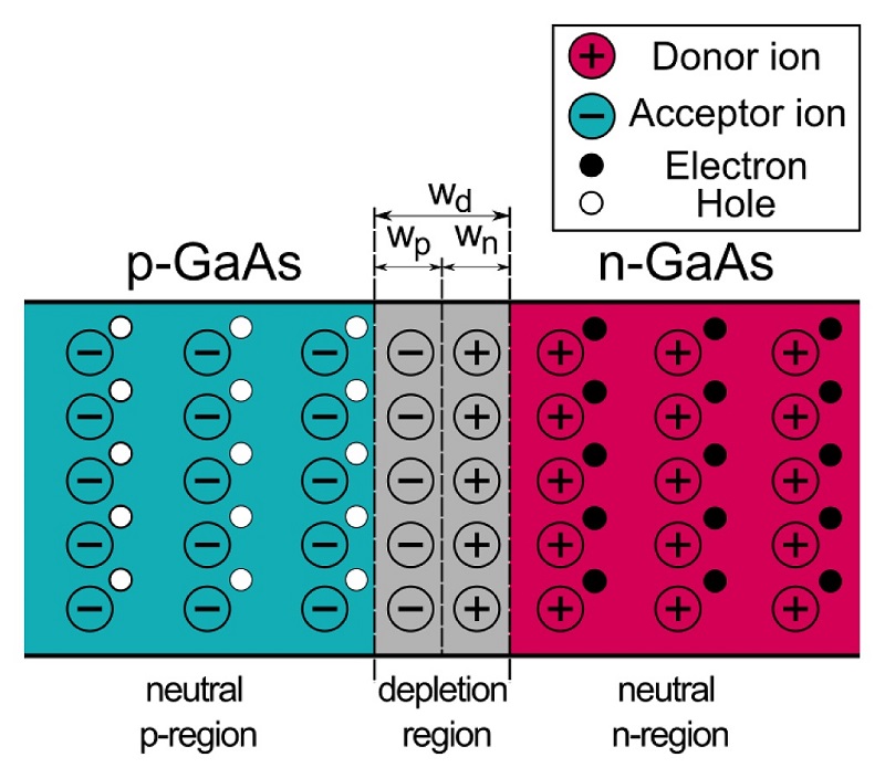
Figure 5.3.3.1 The schematic illustration of the p-n junction.
At equilibrium, the built-in-potential \(V_{bi}\) is formed across the space charge region. The process of forming the built-in-potential is explained below. First, the carrier density gradients arise across the junction when p-doped GaAs and n-doped GaAs are joined. Then, the free electrons in n-doped GaAs diffuse and combine with holes in p-doped GaAs. Similarly, the free holes in p-doped GaAs diffuse and combine with electrons in n-doped GaAs. On the other hand, the ionized dopants, such as negatively charged acceptor and positively charged donor, cannot move and are fixed at their initial positions. Therefore, the ionized dopants in the region where the carriers are depleted form the electric field and the built-in-potential \(V_{bi}\) that impede the diffusion of majority carriers. The space charge region (the width: \(w_{d}\)) denotes the region that is charged and loses the mobile carriers.
Figure 5.3.3.2 shows the basic characteristics of the diode at equilibrium.

Figure 5.3.3.2 Some characteristics are shown across a p-n junction. (a) shows the dopant profile. (b) and (c) are the electric field and the potential across the space charge region, respectively.
Note that we assume the all dopants are ionized in the result to be consistent with Fig. 6.3. in [NelsonPSC2003]. You can see that the electric field is formed within the space change region and the voltage is equivalent to \(V_{bi}\) from Figure 5.3.3.2 (b) and (c).
Figure 5.3.3.3 shows (a) the band profiles and (b) the carrier densities at equilibrium. bandedges.dat, density_electon.dat, and density_hole.dat are used to produce this figure.

Figure 5.3.3.3 The band profiles are plotted in (a). The carrier densities are plotted in (b). The hole density is shown in violet, whereas the electron density is in green.
In (a), \(\mathrm{CB}\) and \(\mathrm{VB}\) represent conduction and valence band, respectively. \(\mathrm{E}_{Fn}\) and \(\mathrm{E}_{Fp}\) are the electron quasi Fermi level and the hole quasi Fermi level. The results are in a good agreement with Fig. 6.5. in [NelsonPSC2003].
\(V_{bi}\) can be calculated at potential.dat and it is \(2.7848 - 1.5779 = 1.207\;\mathrm{V}\) in this case. The width of the space charge region \(w_{scr}\) can be acquired by the following procedures.
Since
and
Thus,
Each parameter corresponds to a value in the table below.
Parameter |
Value |
|---|---|
\(q\) (Elementary charge) |
\(1.6022\times10^{-19}\;\mathrm{C}\) |
\(\varepsilon_{0}\) (Vacuum permittivity) |
\(8.854\times10^{-12}\;\mathrm{C/(Vm)}\) |
\(\varepsilon\) (Relative permittivity of GaAs) |
\(12.93\) |
\(N_{a}\) |
\(1.0\times10^{17}\;\mathrm{cm^{-3}}\) |
\(N_{d}\) |
\(1.0\times10^{16}\;\mathrm{cm^{-3}}\) |
Thus, \(w_{scr}\) is:
From the equation (5.3.3.3), you can see that the higher the dopant concentration is, the thinner \(w_{scr}\) becomes.
The derivation of the equations is explained in \(\S6\) in [NelsonPSC2003].
Under applied bias
We look into the case of the diode under forward bias. Figure 5.3.3.4 shows animation of (a) the band profiles, (b) the electric field, and (c) the space charge, respect to the applied bias.
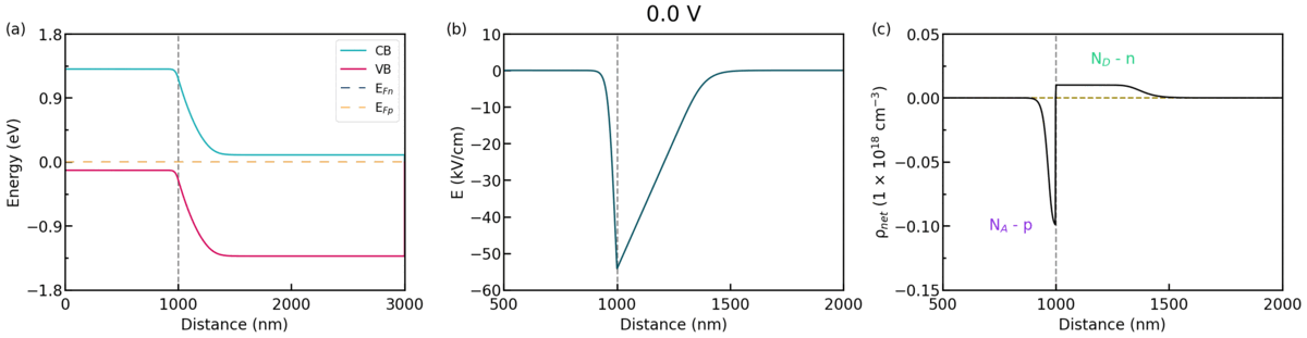
Figure 5.3.3.4 Some characters, (a) the band profiles, (b) the electric field, and (c) the space charge, respect to the applied bias.
As you see in Figure 5.3.3.4, the width \(w_{scr}\) decreases as the forward bias is applied. The width \(w_{scr}\) under the forward bias can be represented as follows.
As the width \(w_{scr}\) decreases, the electric field that prevents the diffusion of majority carriers also decreases.
Whereas the current density across the diode is 0 at equilirium, applied bias enables majority carriers to diffuse across the junction. This means that a net current of electrons flow from n to p, and a net current of holes from p to n.
To see the effects of applied bias more clearly, let us look at the band profiles and carrier densities at \(0.5\;\mathrm{V}\).

Figure 5.3.3.5 The band profiles are plotted in (a). The carrier densities are plotted in (b). The hole density is shown in violet, whereas the electron density is in green.
The results are consistent with Fig. 6.6. in [NelsonPSC2003] with high accuracy. The built-in-potential is reduced to \(V_{bi} - V = 1.207 - 0.5 = 0.707\;\mathrm{V}\). Here, the difference between the quasi Fermi levels within the space charge region is equivalent to \(qV\).
Thus,
This relation can be seen from Figure 5.3.3.5 (a).
J-V curve
In this section, we sweep forward bias to acquire J-V curve. You can refer to I–V characteristic of GaAs p–n junction | 1D/2D/3D to understand how to apply bias in nextnano++.
Figure 5.3.3.6 shows the J-V curve of the diode. IV_characteristics.dat is used to produce this figure.

Figure 5.3.3.6 J-V curve of the diode. (i) space charge recombination current region, (ii) diffusion current region, (iii) high-injection region, (iv) series-resistence effect region.
The light-blue curve shows the numerical result in nextnano++. The violet and orange dashed-dotted curves are acquired analytically. They correspond to \(J_{scr}\) and \(J_{diff}\) in Fig. 6.7. in [NelsonPSC2003], respectively.
\(J_{scr}\) is called the recombination current density and expressed in the following equation:
where
\(J_{diff}\) is called the diffusion current density and expressed in the following equation:
where
The parameters used in the expressions above are in the table.
Parameters |
Description (unit) |
Value used for the analytical J-V curve |
|---|---|---|
\(k_{B}\) |
Boltzmann constant (J/K) |
1.3806E-23 |
\(T\) |
The temperature (K) |
300 |
\(n_{i}\) |
The intrinsic carrier density (cm-3) |
2.318E+6 |
\(\tau_{n/p}\) |
The lifetimes of electrons/holes (s) |
3.333 \(\times\) 10-9 for \(J_{scr}\) and 1.0 \(\times\) 10-10 for \(J_{diff}\) (*) |
\(D_{n/p}\) |
The diffusion coefficients of electrons/holes (cm2/Vs) |
219.73 / 20.681 |
\(L_{n/p}\) |
The diffusion lengths of electrons/holes (cm) |
1.4823 \(\times\) 10-4 / 4.5476 \(\times\) 10-5 |
Attention
- (*) There seems to be some errors related to the units in Fig. 6.7. in [NelsonPSC2003]
Therefore we used the lifetimes as fittig parameters.
The derivation of those equations above are described in \(\S6\) in [NelsonPSC2003]. \(J_{a}\) is the sum of \(J_{scr}\) and \(J_{diff}\) (\(J_{a} = J_{scr} + J_{diff}\)). Our result (the light-blue curve) is in a good agreement with \(J_{a}\) until \(V \approx 1.2\;\mathrm(V)\).
Our result shows the four distinct regions as marked Figure 5.3.3.6 (region (i), (ii), (iii), (iv)). In the next section, we identify the origins of the appearance of the regions.
Recombination current region
The region (i) is attributed to the recombination current region, where the contribution of \(J_{scr}\) is dominant. In this region, electrons and holes recombine within the space charge region since the region still exists. Therefore, the recombination current flows to compensate externally for the disappearance of the recombined carriers. As you can see from (5.3.3.6), in the semi-log plot \(log(J)\; vs\; V\), the slope in the region (i) is \(qV/2k_{B}T\).
Diffusion current region
The region (ii) is the diffusion current region. The contribution of \(J_{diff}\) is large in this region. Since the space change region almost disappears, a large amount of carriers starts to diffuse. This means that electrons are injected into p-doped GaAs and holes are injected into n-doped GaAs (minority carriers injection). As you can see from (5.3.3.8), in the semi-log plot \(log(J)\; vs\; V\), the slope in the region (ii) \(qV/k_{B}T\).
High-injection region
With increasing the forward bias towards \(V_{bi}\), the injected hole density becomes comparable to the electron density at the n-side of the junction. You can see it in Figure 5.3.3.7 (b), where \(1.2\;\mathrm{V}\) is applied to the diode.

Figure 5.3.3.7 The band profiles are plotted in (a). The carrier densities are plotted in (b). The hole density is shown in violet, whereas the electron density is in green.
Then, the electron density must increase to maintain the neutrality. As a result, \(n \approx p\) holds.
Because of the law of the junction,
we acquire the equation as follows.
Therefore, the current density becomes roughly proportional to \(\exp(qV/2k_{B}T)\).
Series-resistance effect
At large currents, the voltage drop outside the space charge region becomes too large to ignore. This is equivalent to considering a single resistance (\(R\)) added in series to the ideal diode and corresponds to the region (iv). In this region, the diffusion current density becomes proportional to the applied voltage to the diode (\(V^*\)).
where
Numerical control
Since we solve the current equation and the poisson equation (explanation: Photocurrent and Efficiencies) self-consistently, we need some techniques to make the calculations more stable.
In this section, we introduce the effects of minimum_density_electrons, minimum_density_holes, maximum_density_electrons, and maximum_density_holes.
You should also check Convergence.
In Figure 5.3.3.6, we divide the simulation scheme into 3, depending on the magnitudes of minimum and maximum carrier densities (scheme (A), (B), and (C)). Scheme (A): \(0 \sim 0.4\;\mathrm{V}\) Scheme (B): \(0.4 \sim 0.7\;\mathrm{V}\) Scheme (C): \(0.7 \sim 1.5\;\mathrm{V}\)
First, the code below defines the magnitudes of the minimum and maximum carrier densities.
Note that we use the variables $min_density and $max_density for convenience.
178currents{
179    minimum_density_electrons  = $min_density
180    minimum_density_holes      = $min_density
181    maximum_density_electrons  = $max_density
182    maximum_density_holes      = $max_density
183
184}
Usually, you can set the values of $min_density_* and $max_density_* by referring to bias_XXXXX\density_electon.dat and bias_XXXXX\density_hole.dat.
In the scheme (C), the maximum electron and hole densities are about \(1.0\times10^{18}\;(\mathrm{cm^{-3}})\).
Therefore, it is set to 1.0E+20.
Similarly, you can set $minimum_density_*.
Since the minimum electron and hole densities are about \(1.0\times10^{0}\;(\mathrm{cm^{-3}})\), $minimum_density_electrons = 1.0E-2 and $minimum_density_holes = 1.0E-2 are enough low to evaluate the current density accurately.
Note that \(x = 0\;\mathrm(nm)\) and \(x = 3000\;\mathrm(nm)\) correspond to the positions of the interfaces of diode/contact.
Therefore, we do not include the carrier densities at the positions into the procedures.
In the scheme (B), $minimum_density_electrons = 1.0E-2 and $minimum_density_holes = 1.0E-2 is enough low as well.
However, you have to take care of the magnitude of $minimum_density_*.
Figure 5.3.3.8 (a) shows the effect of the magnitude of $minimum_density_* on the current density under \(0.5\;\mathrm{V}\) in the scheme (B).

Figure 5.3.3.8 The effect of the magnitude of $minimum_density_* on the current density. (a) is under \(0.5\;\mathrm{V}\) in the scheme (B). (b) is under \(0.1\;\mathrm{V}\) in the scheme (A).
Although the current density has to be constant through the diode, it becomes unstable at minimum_density_* set to 1.0E+16 and minimum_density*_ set to 1.0E+20.
Thus, you should set $minimum_density_* to 1.0E+15, which shows the constant current density.
In the scheme (A), the same techniques should be applied.
Figure 5.3.3.8 (b) shows the effect of the magnitude of $maximum_density_* on the current density under \(0.1\;\mathrm{V}\) in the scheme (A).
As you can see, maximum_density_* should be set to 1.0E+12 to keep the current density constant through the diode.
Exercises
under construction
Last update: 2025-10-16