
— DEV — I–V characteristics of n-doped Si structure#
- Input files:
I-V_n-doped-Si_1D_nnp.in
I-V_n-doped-Si_2D_nnp.in
I-V_n-doped-Si_3D_nnp.in
I-V_nin-doped-Si_1D_nnp.in
I-V_nin-doped-Si_2D_nnp.in
I-V_nin-doped-Si_3D_nnp.in
- Scope:
This tutorial aims to simulate the I-V characteristics of n-doped and n-i-n doped Si structures.
- Output files:
IV_characteristics.dat
bias_xxxxx/bandedges.dat
I-V characteristics of an n-doped Si structure#
Structure#
The structure we are dealing with consists of bulk Si that is sandwiched between two contacts. The whole structure has the following dimensions (see also):
along \(x\)-axis: \(20\,\mathrm{nm}\) (\(1\,\mathrm{nm}\) contact, \(18\,\mathrm{nm}\) Si, \(1\,\mathrm{nm}\) contact)
along \(y\)-axis: \(5\,\mathrm{nm}\)
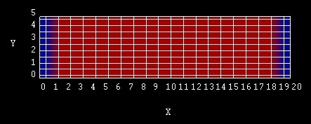
Figure 179 Simulated structure consisting of a left and right contact (blue) and n-doped Si layer (red).#
The Si is n-type doped with a donor concentration of \(N_\mathrm{D} = 1\cdot 10^{20}\,\mathrm{cm^{-3}}\). The energy level is 0.044 eV below the conduction band edge. This leads to an electron density of \(n = 13.48 \cdot 10^{18}\,\mathrm{cm^{-3}}\), which corresponds to the concentration of the ionized donors. The Fermi level \(E_\mathrm{F}\) is taken to be at 0 eV in an equilibrium simulation, i.e. \(V = 0\,\mathrm{V}\). The distance of the conduction band from the Fermi level can be calculated in the following way:
For the effective electron mass at the \(\Delta\)-point we have:
where \(m_\mathrm{l}\) is the longitudinal and \(m_\mathrm{t}\) is the transversal mass of the effective mass tensor.
The effective density of states reads:
where the factor of 12 arises due to the six-fold degeneracy of Si at \(\Delta\) and the two-fold spin degeneracy. Similarly, we obtain the effective density of states for holes:
Note that heavy and light holes are degenerate for \(k = 0\), i.e. \(N_\mathrm{v} = N_\mathrm{v,\,hh} + N_\mathrm{v,\,lh} = 1.1377\cdot 10^{19}\,\mathrm{cm^{-3}}\).
The Semiconductor equation is given by
with \(E_\mathrm{gap} = 1.095\,\mathrm{eV}\), \(n_\mathrm{i} = 1.113\cdot 10^{10}\mathrm{cm^{-3}}\) and \(p = n_\mathrm{i}^2/n = 9.185\,\mathrm{cm^{-3}}\).
The occupation of the different energy states can either be described by Maxwell-Boltzmann statistics:
or Fermi-Dirac statistics:
where \(\mathcal{F}_{1/2}\) is the Fermi-Dirac integral of order \(1/2\) multiplied by the factor \(2/\sqrt{\pi}\) (i.e. \(\mathcal{F}_{1/2}\) includes the Gamma pre-factor)
When using the Maxwell-Boltzmann statistics as an approximation, we obtain:
Note that nextnano++ uses the Fermi-Dirac integrals (Fermi-Dirac statistics), where the following results are obtained: \(E_\mathrm{c}=13.85\,\mathrm{meV}\) and \(E_\mathrm{v} = -1.0815\,\mathrm{eV}\).
Results#
We sweep the voltage at the right contact from \(0.0\,\mathrm{V}\) to \(0.2\,\mathrm{V}\) in 10 steps. The input files used for the simulations are I-V_n-doped-Si_1D_nnp.in, I-V_n-doped-Si_2D_nnp.in I-V_n-doped-Si_3D_nnp.in. The calculated current density for each bias point can be found in IV_characteristics.dat. The resulting I-V characteristics is depicted in Figure 180.
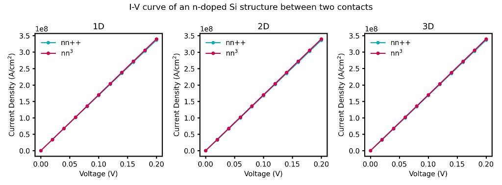
Figure 180 Simulated I-V characteristics of an n-doped Si structure using constant mobility model.#
The nextnano++ results are in agreement with the I-V characteristics obtained with nextnano³. The units for the current in a 2D simulation are [\(\mathrm{A/m}\)]. Dividing this two-dimensional current value by the width of the device (in our case 5 nm) we obtain the current in units of [\(\mathrm{A/cm^2}\)], which is the usual unit of a 1D simulation. As our simple 2D example structure is basically equivalent to a 1D structure we can easily compare our 2D results with the 1D results to check for consistency. It is also possible to perform a 3D simulation. In this case, the units for the three-dimensional current are [\(\mathrm{A}\)]. Dividing by the area of the device of \(25\,\mathrm{nm^2}\), we obtain the 1D units of [\(\mathrm{A/cm^2}\)].
I-V characteristics of an n-i-n-doped Si structure#
Structure#
The second example is an n-i-n (n-doped, intrinsic, n-doped) Si structure, which is shown in Figure 181. The width of the intrinsic region is 14 nm, and the n-doped regions are both 2 nm wide.
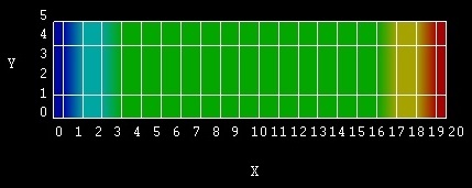
Figure 181 Simulated n-i-n structure consisting of a left contact (dark blue), n-doped Si (light blue), intrinsic Si (green), n-doped Si (yellow) and right contact (red).#
Results#
In Figure 182 the current-voltage (I-V) characteristic is shown. The input files used for the simulations are I-V_nin-doped-Si_1D_nnp.in, I-V_nin-doped-Si_2D_nnp.in I-V_nin-doped-Si_3D_nnp.in. The data of the I-V curve can be found in the corresponding file IV_characteristics.dat.
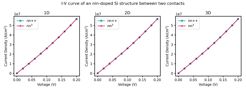
Figure 182 Simulated I-V characteristics of the n-i-n doped Si structure using constant mobility model.#
In order to compare the results from 1D, 2D and 3D simulations, we have divided the 2D current by the width of the device (in our case 5 nm) and the 3D current by the cross-section area of the device of (in our case \(25\,\mathrm{nm^2}\)), to get the current density in units of [\(\mathrm{A/cm^2}\)]. The obtained results are in perfect agreement.
Figure 183 shows the conduction band profile (bias_xxxxx/bandedges.dat) for different voltages.
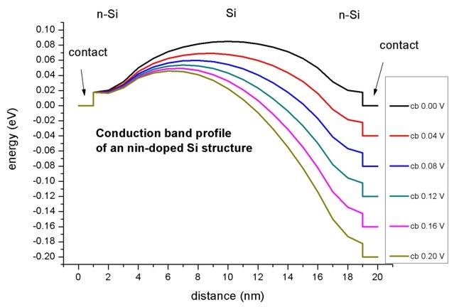
Figure 183 Simulated conduction band profile of the n-i-n Si structure for different voltages.#
Last update: 17/07/2024