3.3.4. HgTe/CdTe Quantum Well
- Input files:
1D_HgTe_CdTe_QW_TBcomparison_kp.nn3
1D_HgTe_CdTe_QW_TBcomparison_TB.nn3
1D_HgTe_CdTe_QW_TBcomparison_kp_QWwidth_Novik.nn3
- Database files:
TB_distance_parameters_no_strain_HgTeCdTe.in
TB_material_parameters_no_strain_HgTeCdTe.in
This tutorial presents simulation of HgTe/CdTe quantum wells with description as in [BirnerPhD2011].
Note
The tight-binding parameters are the same as our default tight-binding database (TB_material_parameters_in). The distance parameters are different (TB_distance_parameters.in) because we do not include strain here. For simplicity, and to be consistent to the paper of [Novik2005], we do not include strain although strain is supported in our software.
HgTe is an interesting material for studies of the intrinsic spin Hall effect [Brüne2010] and the quantum spin hall effect [Bernevig2006], or spin splitting effects in general due to its large Rashba-type spin-orbit splitting. HgTe is a zero-gap semiconductor that can be embedded between CdTe layers to form a HgTe-CdTe quantum well (QW) heterostructure which shows an interesting type-III band alignment where the valence band edge in the HgTe QW lies above its conduction band edge. Due to this band alignment it is not possible to apply a single-band Hamiltonian. Thus a \(\mathbf{k} \cdot \mathbf{p}\) or tight-binding approach is required. Large HgTe quantum wells have an inverted band structure where the highest hole state (h1) lies above the lowest electron state (e1). For smaller quantum well widths, the quantum confinement increases and below a critical well width, the band structure becomes normal again with the electron state above the hole state. Figure 3.3.4.1 shows the square of the calculated \(\mathbf{k} \cdot \mathbf{p}\) wave functions of e1and h1at the crossover well width at 6.5 nm. Increasing the well width shifts the e1 state below the h1 state. This is shown in Figure 3.3.4.2 where the probability density of the relevant states have been calculated with the empirical tight-binding method for a 7.8 nm HgTe quantum well. One can nicely see that in the tight-binding method the envelope of the probability density corresponds to \(\mathbf{k} \cdot \mathbf{p}\) envelope functions. For the sp3d5s* tight-binding [JancuPRB1998] calculations, we used a valence band offset of 0.4 eV. For the \(\mathbf{k} \cdot \mathbf{p}\) calculations, we took exactly the same material parameters as in Ref. [Novik2005], including their valence band offset of 0.570 eV. In both cases, we neglected strain effects for simplicity.
Figure 3.3.4.3 shows the energies of the electron and hole states in a HgTe-CdTe quantum well as a function of HgTe QW width calculated with the 8-band \(\mathbf{k} \cdot \mathbf{p}\) method. The crossover of normal to inverted band structure occurs around 6.5 nm and corresponds to the situation in Figure 3.3.4.1. The dashed lines indicate the energetic positions of the conduction and valence band edges of the HgTe QW. Our results for the crossover width are in good agreement to the calculations of Novik et al. [Novik2005], and also close to tight-binding calculations. I have implemented Peter Vogl’s TIGHTEN superlattice code into the nextnano³ software package, so that it is now more convenient to perform systematic comparisons between the \(\mathbf{k} \cdot \mathbf{p}\) and the tight-binding method for quantum wells.
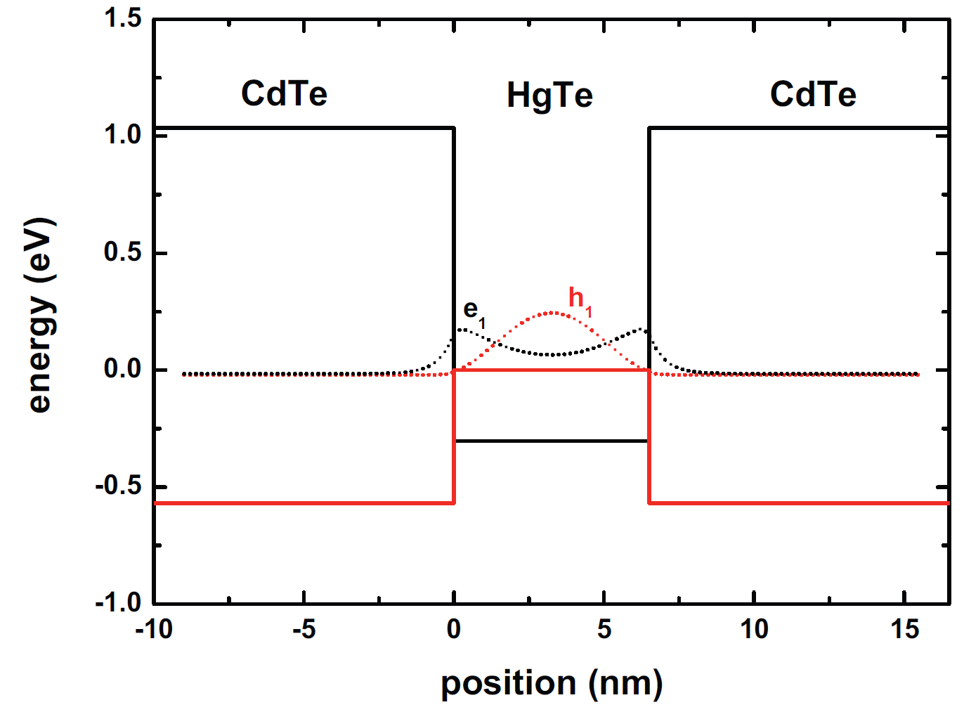
Figure 3.3.4.1 Probability density of the lowest electron (e1) and highest hole (h1) eigenstates of a 6.5 nm HgTe quantum well calculated with the \(\mathbf{k} \cdot \mathbf{p}\) method. In the \(\mathbf{k} \cdot \mathbf{p}\) method, the eigenstates correspond to envelope functions. The conduction (black solid line) and valence band edges (red solid line) form a type-III band alignment.
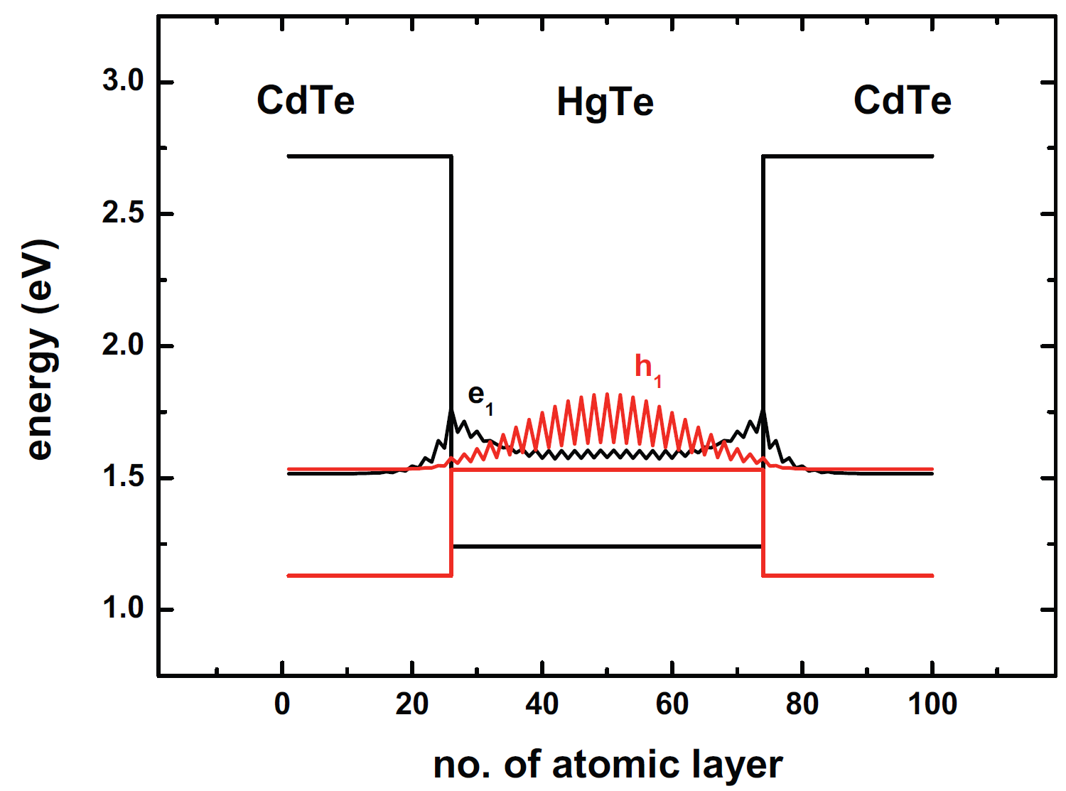
Figure 3.3.4.2 Probability density of the lowest electron (e1) and highest hole (h1) eigenstates of a 7.8 nm HgTe quantum well calculated with the empirical tight binding method.
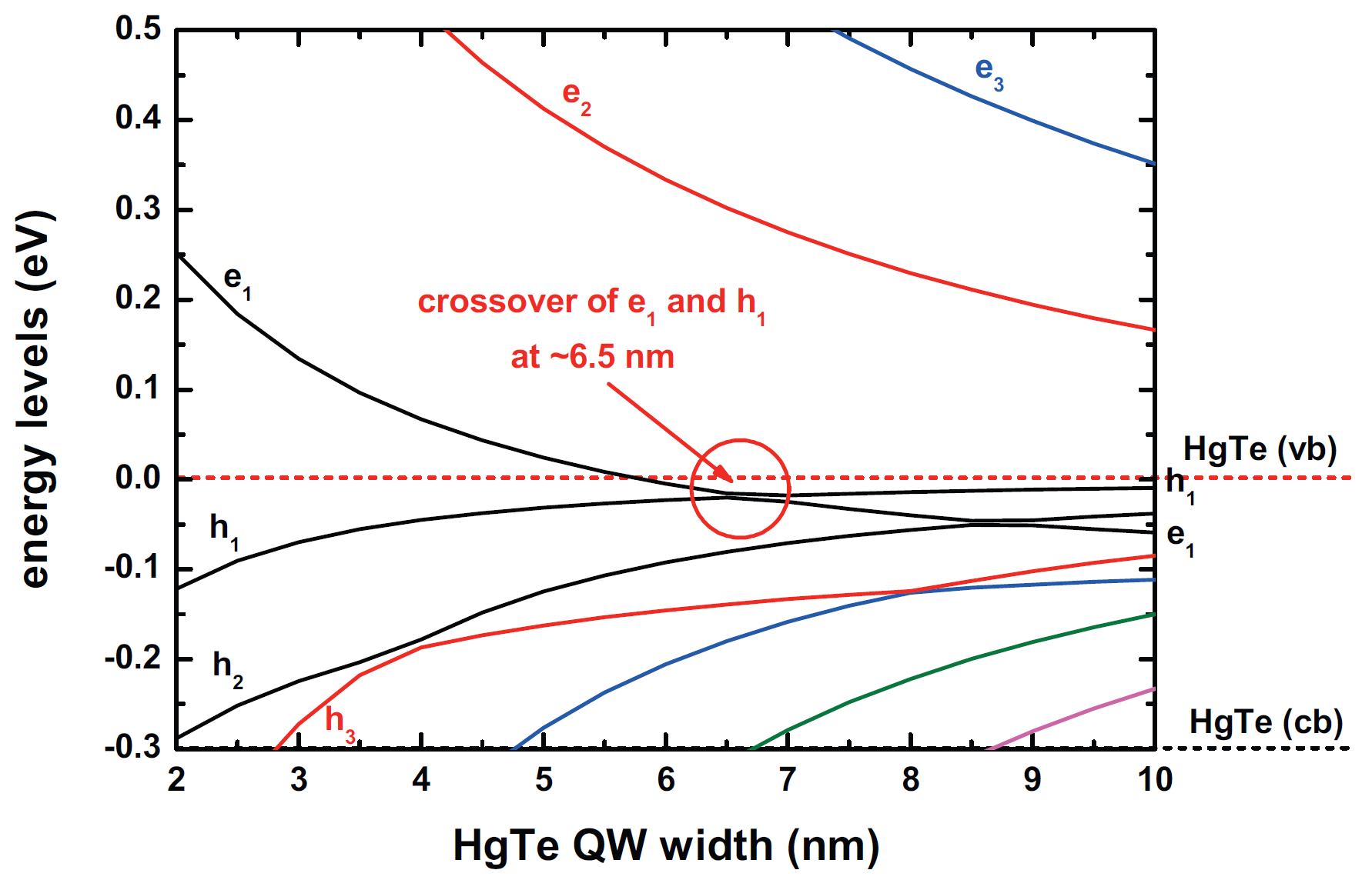
Figure 3.3.4.3 Calculated energies of the electron and hole states in a HgTe-CdTe quantum well as a function of HgTe QW width (8-band \(\mathbf{k} \cdot \mathbf{p}\)). The crossover of normal to inverted band structure occurs around 6.5 nm and corresponds to the situation in Figure 3.3.4.1. The dashed lines indicate the conduction and valence band edges of the HgTe QW.