|
| |
nextnano3 - Tutorial
next generation 3D nano device simulator
1D Tutorial
InAs / GaSb broken gap quantum well (BGQW) (type-II band alignment)
Author:
Stefan Birner
-> 1DInAs_GaSb_BGQW_k_zero_nn3.in       /
*_nnp.in
-
input file for the nextnano3 and nextnano++ software
-> 1DInAs_GaSb_BGQW_k_parallel_nn3.in   / *_nnp_01.in / *_nnp_11.in
-
These input files are included in the latest version.
InAs / GaSb broken gap quantum well (BGQW) (type-II band alignment)
This tutorial aims to reproduce Figs. 1, 2(a), 2(b) and 3 of
Hybridization of electron, light-hole, and heavy-hole states in
InAs/GaSb quantum wells
A. Zakharova, S.T. Yen, K.A. Chao
Physical Review B 64, 235332 (2001)
The material parameters were taken from
Optical transitions in broken gap heterostructures
E. Halvorsen, Y. Galperin, K.A. Chao
Physical Review B
61 (24), 16743 (2000)
The heterostructure is a broken gap quantum well (BGQW) with 15 nm InAs and 10
nm GaSb, sandwiched between two 10 nm AlSb layers.
Note that this heterostructure is asymmetric.
To be consistent with the above cited papers, strain is not included into the
calculations although this would be possible.
The structure has a type-II band alignment, i.e. the electrons are
confined in the InAs layer,
whereas the holes are confined in the GaSb layer.
Depending on the width of the InAs and/or GaSb layers, things can be even more
complicated because the hole states can hybridize with the electron states,
making it difficult to distinguish between electron-like and hole-like states.
Another difficulty arises because the lowest electron states might be located
below the highest hole states. This requires a new algorithm to occupy the
states according to a suitable Fermi level.
The following figure shows the electron and hole band edges of the BGQW
structure.
- band_structure/cb1D_001.dat (Gamma conduction
band edge) in units of [eV]
- band_structure/vb1D_001.dat (heavy hole
valence band edge) in units of [eV]
- band_structure/vb1D_002.dat (light
hole valence band edge) in units of [eV]
- band_structure/vb1D_003.dat (split-off hole valence
band edge) in units of [eV]
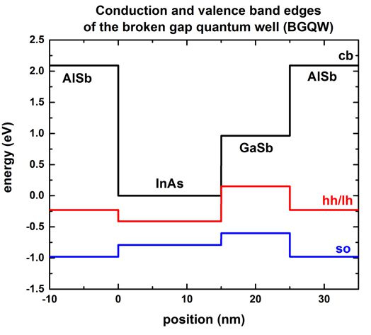
The origin of the energy scale is set to the InAs conduction band edge energy.
The heavy hole and light hole band edges are degenerate because we neglect the
effects of strain to be consistent with the above cited papers.
Results
-
-> 1DInAs_GaSb_BGQW_k_zero.in
The following figure shows the conduction band edge and the heavy/light hole valence band edges in this
BGQW structure
together with the electron (e1, e2), heavy hole (hh1,
hh2, hh3)
and light hole (lh1) energies and
wave functions (psi²), calculated within 8-band k.p theory at the zone
center, i.e. at k|| = 0.
One can clearly see that the electron state (e1,
e2) are confined in the
InAs layer (left part of the figure),
whereas the heavy (hh1,
hh2, hh3) and light hole (lh1)
states are confined in the GaSb layer (right part
of the figure).
One can see a slight hybridization of the e1 and lh1
states, i.e. these states are mixed states whereas the heavy hole states (hh1,
hh2, hh3) are not mixed and
thus confined in the GaSb layer.
- Schroedinger_kp/kp_8x8psi_squared_qc001_el_kpar0001_1D_dir.dat
- contains Psii2
- Schroedinger_kp/kp_8x8psi_squared_qc001_el_kpar0001_1D_dir_shift.dat -
The latter file contains the square of the wave functions (for kpar0001,
i.e k|| =
0, i.e. kx = ky = 0), shifted by their energies, so that
one can nicely plot the conduction and valence band edges together with the
square of the wave functions.
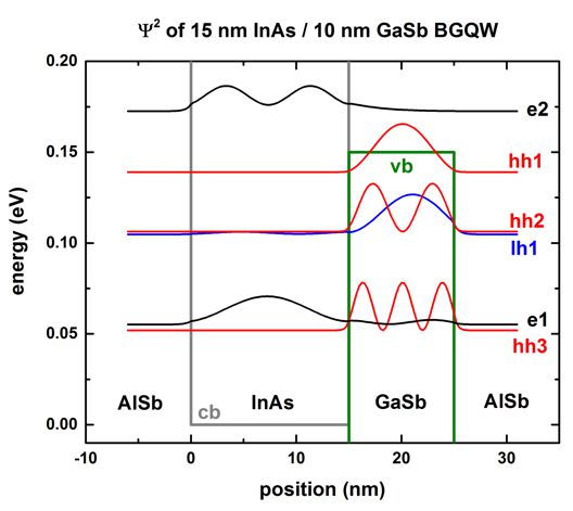
The energies of the eigenstates are in units of [eV] and are contained in
this file:
- Schroedinger_kp/kp_8x8eigenvalues_qc001_el_kpar0001_1D_dir.dat.dat
-> 1DInAs_GaSb_BGQW_k_parallel.in
The following figure shows the E(k||) dispersion of the
electron and hole states along the [10] direction and along the [11] direction in (kx,ky) space.
The [01] direction has the same dispersion due to symmetry arguments.
In this input file, the energy levels and wave functions for 24 k||
points along a line from (kx,ky) = (0,0) to (kx,ky)
= (0,ky) have been calculated.
- Schroedinger_kp/kpar1D_disp_01_00el_8x8kp_ev_min001_ev_max020.dat
contains the k|| dispersion from [00] to [01] because
in the input file it is specifed:
	$output-kp-data

     !k-par-dispersion = 01-00      !
k-par-dispersion = 01-00-11 !
...ev_min001_ev_max020...)
i.e. to include lines ("lines are a guide to the eye").
The black lines are the results of
the nextnano++ software, the red dots
are the results of the nextnano3 software.
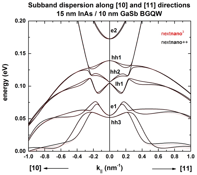
At an in-plane wave vector of 0.014 1/Angstrom, strong intermixing between the
e1 and the lh1 states occurs.
In contrast to the wave functions at k|| = 0, where the e1
and lh1 wave functions are nearly purely electron- or hole like, the
wave functions at k|| = (0,0.014) = (0.014,0) are a
mixture of electron and light hole wave functions. Compare with Fig. 4 of the
A. Zakharova et al.
In asymmetric quantum wells, the double spin degeneracy is lifted at finite
values of k|| because of spin-orbit interaction. This is
the reason why we have two different dispersions E(k||)
for "spin up" and "spin down" states.
This also means that the wave functions at finite k|| are
different for "spin up" and "spin down" states.
- The file
Schroedinger_kp/kp_8x8k_parallel_qc001_el1D_dir.dat
tells us which number of k|| vector corresponds to (kx,ky).
   k_par_number   k_x [1/nm]
	k_y [1/nm]

	     1
	0.000000E+000   0.000000E+000     ==>
k|| = (kx,ky) = (0,0)
	[1/nm]

     ...

	     29
	0.000000E+000   1.400000E+000
==> k|| = (kx,ky)
= (0,0.14) [1/nm]
1326
1.00000E+000 1.000000E+000 ==>
k|| = (kx,ky) = (1.0,1.0)
[1/nm]
- In the following figure, we plot the square of the wave functions for k|| = (0,0.14) nm-1.
The corresponding label of our k|| numbering is
29. Note that this labeling depends on
the k|| space resolution, i.e. the number of k||
points that have been specified in the input file: num-kp-parallel =
10000
The wave functions are contained in this file:
- Schroedinger_kp/kp_8x8psi_squared_qc001_hl_kpar00029_1D_dir_shift.dat - contains
Psii2 + Ei
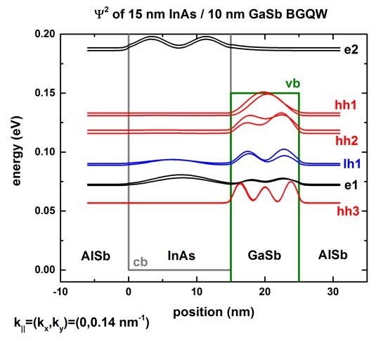
The electron states (e1)
couple strongly with the light hole states (lh1).
This is expected from the energy dispersion plot because at 0.14 nm-1
a strong anticrossing is present for these states.
One can also clearly see that for spin up and spin down states, different
energy levels and different probability densities exist.
This is in contrast to the states at k|| = 0 which are
two-fold spin degenerate as shown in the figure further above.
Our results are similar to Fig. 4 of Zakharova's paper.
|