| nextnano.com nextnano³ Download | Search | Copyright | Publications * password protected |
nextnano³ software
|
|
| 1D nin Si resistor |
|
|
|
|
|
nextnano3 - Tutorialnext generation 3D nano device simulator1D Tutorialn-i-n Si resistorAuthor: Stefan Birner If you want to obtain the input file that is used within this tutorial, please
submit a support ticket. This tutorial is based on the example presented on p. 43 in Stefan Hackenbuchner's PhD thesis, TU Munich (2002) and on the following paper:
n-i-n Si resistor
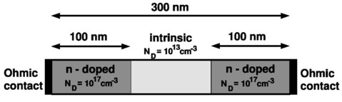
Here, we illustrate our method for calculating the current by studying simple one-dimensional examples that we can compare to full Pauli master equation results. Our method amounts to calculating the electronic structure of a device fully quantum mechanically, yet employing a semi-classical scheme for the evaluation of the current. As we shall see, the results are close to those obtained by the full Pauli master equation provided we limit ourselves to situations not too far from equilibrium. We consider a one-dimensional 300 nm Si-based n-i-n resistor at room temperature, where "n-i-n" stands for "n-doped / intrinsic / n-doped". The intrinsic region and the n-doped regions are each 100 nm wide.
The figure shows the geometry of the n-i-n Si resistor. The n-doped regions at the left and right sides are doped with a doping
concentration of ND = 1 x 1017 cm-3.
For a more detailed discussion of this equation (including Fermi-Dirac statistics), please read the description in Tutorial "I-V characteristics of an n-doped Si structure". At both ends of the device there are ohmic contacts. The conductivity electron mass is given by
whereas the DOS electron effective mass is given by
The static dielectric constant is given by epsilon = 11.7. For the donors we assumed an ionization energy of 0.015 eV as well as a degeneracy factor of 2. For the mobility which should depend on the electric field and on the
concentration of ionized impurities we assumed
The electron density in nextnano³ can be calculated in two ways:
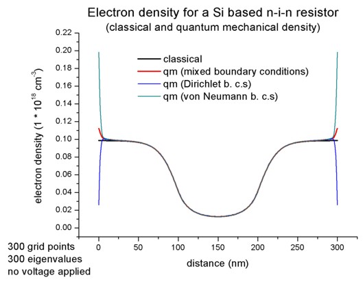
Classical and quantum mechanical electron densities at equilibrium, i.e. applied bias = 0 VNow let us first have a look at the electron densities for the cases of The electron density is the sum over all three valleys (Gamma point, L point and X point (or Delta for Si) in the Brillouin zone) whereas for Si the dominant valley is the X valley which is sixfold degenerate (or twelvefold degenerate including spin degeneracy). Thus we solve Schrödinger's equation only in the X valley and take for the other valleys the classical density only. For b) we have to choose appropriate boundary conditions where we choose
"mixed". (Note: The feature of using "mixed" boundary conditions
for the Schrödinger equation is not supported any more.) For comparison we also show the results of Dirichlet and Neumann
boundary conditions although we do not recommend the latter for current
calculations.
To switch off the current calculation, we have to choose: In the following figure we compare for 0 V applied bias, i.e. for equilibrium where no current flows, the classical and the quantum mechanical electron densities.
Classical and quantum mechanical electron densities for the n-i-n resistor. Dirichlet boundary conditions force the wave function to be zero at the boundaries and thus the electron density is zero as well. Thus to get a meaningful and physical electron density at the boundaries we have to choose "mixed" boundary conditions. (Note: The feature of using "mixed" boundary conditions for the Schrödinger equation is not supported any more.)
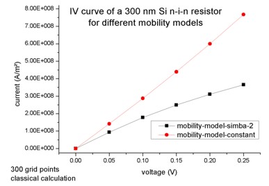
Current-voltage characteristics of the Si n-i-n resistorNow we vary the applied bias in steps of 0.05 V (
IV characteristics of the 300 nm Si n-i-n resistor for two different mobility models (classical simulations).
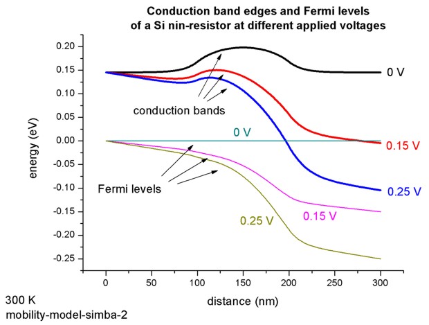
The conduction band edges and the Fermi levels (i.e. chemical potentials) for
the electrons at different applied voltages are plotted in this figure:
Quantum mechanical calculations
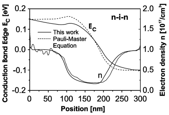
As one may expect, true quantum mechanical effects play little role in this case and both the nextnano³ (i.e. the semi-classical drift-diffusion) and the Pauli master equation approach yield practially identical results for the density and conduction band edge energies (i.e. for the electrostatic potential). We would like to point out that this good agreement is a nontrivial finding, as we calculate the density quantum mechanically with self-consistently computed local quasi-Fermi levels rather than semi-classically. The following figure shows for an applied bias of 0.25 V the conduction band edge energies and the electron densities. One can see that our results agree very well with the solution of the Pauli master equation (M.V. Fischetti, J. Appl. Phys. 83, 270 (1998)). Fischetti obtains for the current density 6.8 * 104 A/cm² whereas we obtain 3.65 * 104 A/cm² by using a (semi-)classical drift-diffusion model. However, we note that the current is directly proportional to the mobility in our model, i.e. changing the mobility therefore changes the value of the current but does not affect the electron density or potential profile (is this really true?). If we had chosen a constant mobility of µ = 1417 cm²/Vs then the current at 0.25 V applied bias had been 7.67 * 104 A/cm² (compare with I-V characteristics above).
The figure shows the calculated conduction band edges Ec and the electron densities n of the n-i-n structure as a function of position inside the structure. The results obtained from the Pauli master equation (Fischetti (1998), dashed lines) are compared to our quantum mechanical results (full lines). First one could think that the good agreement between the two approaches is trivial, as quantum mechanical effects do not play any role in this example. However, we want to stress that the electron density was calculated fully quantum mechanically with self-consistent local quasi-Fermi levels. Conclusion Here, we demonstrated our approach to calculate the electronic structure in nonequilibrium where we combine the stationary solutions of the Schrödinger equation with a semi-classical drift-diffusion model. For the electrostatic potential and the charge carrier density, the method leads to a very good agreement with the more rigorous Pauli master equation approach. In addition, the current can also be described accurately. |
|
|