nextnano3 - Tutorial
next generation 3D nano device simulator
2D Tutorial
Electron and hole wave functions in a T-shaped quantum wire grown by CEO
(cleaved edge overgrowth)
Author:
Stefan Birner
If you want to obtain the input files that are used within this tutorial, please
check if you can find them in the installation directory.
If you cannot find them, please submit a
Support Ticket.
-> 2DTshapedQuantumWireCEO.in
Acknowledgement: The author - Stefan Birner - would like to thank
Robert Schuster from the University of Regensburg for providing the experimental
data and some of the figures.
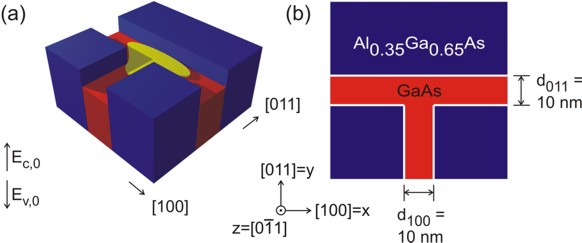
T-shaped quantum wire
Similar to the 1D confinement in a quantum well, it is possible to
confine electrons or holes in two dimensions, i.e. in a quantum wire.
The quantum wire is formed at the T-shaped intersection of two 10 nm GaAs
type-I quantum wells and is confined by Al0.35Ga0.65As barriers.
The electrons and holes are free to move along the z direction only, thus
the wire is oriented along the [0-11] direction. Such a heterostructure can
be manufactured by growing the layers along two different growth directions
with the CEO (cleaved egde overgrowth) technique. Due to the nearly
identical lattice constants of GaAs and AlAs it is possible to assume this
heterostructure as being unstrained.
|
 |
|
The figure on the left shows schematically the conduction band profile of
the T-shaped wire that was grown by the CEO technique. If one inverts the
energy arrow then the left picture corresponds to the valence band edge.
The wave function is indicated at the T-shaped intersection in yellow. Here,
the wave function can extend into a larger volume (as compared to the quantum
well) and thus reduce its energy. So quantum mechanics tells us that the
ground state can be found at this intersection and electrons are only
allowed to move one-dimensionally along the z direction.
The figure on the right shows a 60 nm x 60 nm extract of the schematic layout including the
dimensions, the material composition and the orientation of the wire with
respect to the crystal coordinate system.
|
It is sufficient to describe this heterostructure within a 2D simulation as
it is translationally invariant along the z direction.
The simulation coordinate system is oriented in the following way:
 $domain-coordinates


  domain-type        =
1  1  0  !
  hkl-x-direction-zb = 1  0  0
! [100] direction in the crystal coordinate
system
  hkl-y-direction-zb = 0  1  1
! [011] direction in the crystal coordinate
system
! hkl-z-direction-zb = 0 -1 1 ! [0-11] direction in the crystal
coordinate system
hkl-z-direction does not have to be specified. It
is calculated internally in the code.
The simulations are performed at 4 Kelvin:
 $global-parameters

  lattice-temperature = 4.0d0   !
[K]
Electron, heavy hole and light hole wave functions
The electron and hole wave functions can be calculated within the effective
mass theory (envelope function approximation) by using position dependent
effective masses. In our example, the effective masses are constant within each
material but have discontinuities at the material interfaces. For the electrons,
the effective mass was assumed to be isotropic (conduction band minimum at the
Gamma point) whereas for the heavy and light
holes we used anisotropic effective mass tensors that were derived from the 6-band
k.p parameters (or Luttinger parameters).
The Luttinger parameters for GaAs are given by:
- gamma1 = 6.98
AlAs: 3.76
- gamma2 = 2.06
AlAs: 0.82
- gamma3 = 2.93
AlAs: 1.42
The effective masses of GaAs in units of [m0] can thus be
calculated from these Luttinger parameters for different directions:
- electron (Gamma point):
0.067
AlAs:
0.15
- heavy hole along [100] direction: 1 / ( gamma1 - 2
gamma2 )
=
0.350
AlAs:
0.472
- heavy hole along [011] direction: 1 / ( gamma1 - 1/2 (gamma2
+ 3 gamma3) ) =
0.643
AlAs:
0.820
- light hole along [100] direction: 1 / ( gamma1 + 2
gamma2 )
=
0.090
AlAs:
0.185
- light hole along [011] direction: 1 / ( gamma1 + 1/2 (gamma2
+ 3 gamma3) ) =
0.081
AlAs:
0.159

-
heavy hole isotropic:
1 / ( gamma1 - 0.8 gamma2
- 1.2 gamma3 ) =
0.551
AlAs:
0.

-
light hole isotropic:
1 / ( gamma1 + 0.8 gamma2
+ 1.2 gamma3 ) =
0.082
AlAs:
0.
Usually the database entries for the effective masses assume spherical
symmetry for the holes and are specified with respect to the crystal coordinate
system.
Their default values (isotropic) and the values which were derived from the
Luttinger parameters are given in this table:
| |
heavy hole (GaAs) |
light hole (GaAs) |
|
heavy hole (AlAs) |
light hole (AlAs) |
along [100] direction |
0.350 |
0.090 |
|
0.472 |
0.185 |
along [011] direction |
0.643 |
0.081 |
|
0.820 |
0.159 |
| isotropic |
0.551 |
0.082 |
|
0.714 |
0.163 |
| nextnano³ database (default) |
0.500 |
0.068 |
|
0.5 |
0.26 |
In this tutorial, however, we calculated the effective masses for different
directions and therefore we do not have spherical symmetry anymore.
Thus we have to rotate the new eigenvalues of the effective mass tensors that
are given in the x=[100], y=[011], z=[0-11] simulation coordinate system into
the crystal coordinate system where xcr=[100], ycr=[010],
zcr=[001].
First we have to overwrite the default entries in the database so that they
contain the eigenvalues of the effective mass tensors in the simulation system.
 conduction-band-masses   = 0.067d0
0.067d0  0.067d0 !
...
 valence-band-masses      =
0.350d0  0.643d0  0.643d0 !
eigenvalues of the heavy
hole effective mass tensor [100] [011] [0-11]
0.090d0 0.081d0 0.081d0 !
...
 !
 principal-axes-vb-masses = 1d0      0d0
0d0      !
0d0 1d0 1d0 !
0d0 -1d0 1d0 !
1d0 0d0 0d0 !
0d0 1d0 1d0 !
0d0 -1d0 1d0 !
...
Similar, the valence band masses of AlAs are chosen to be:
 conduction-band-masses   = 0.15d0
0.15d0   0.15d0  !
electron effective
mass (Gamma point) (default)
 valence-band-masses      =
0.472d0  0.820d0  0.820d0 !
0.185d0 0.159d0 0.159d0 !
Further material parameters of relevance:
Conduction band offset Al0.35Ga0.65As / GaAs:
0.2847 eV
Valence band offset Al0.35Ga0.65As
/ GaAs: -0.1926 eV
Egap Al0.35Ga0.65As: 2.2883 eV
Egap GaAs:
1.5193 eV
As we do not have doping and no piezoelectric fields (the structure is
assumed to be unstrained) and as the temperature is assumed to be 4 K, we do not
have to deal with charge redistributions. Thus we can refrain from solving
Poisson's equation and we also do not have to take care about self-consistency.
Both, the heavy hole and the light hole band edge energies are degenerate but
the effective mass tensors differ. Thus we have to solve three Schrödinger
equations, namely for the
- conduction band
- heavy hole band
- light hole band
The lowest hole state is the heavy hole state and the second hole state is the
light hole state. No further hole states are confined. Also, in the conduction
band only the ground state is confined.
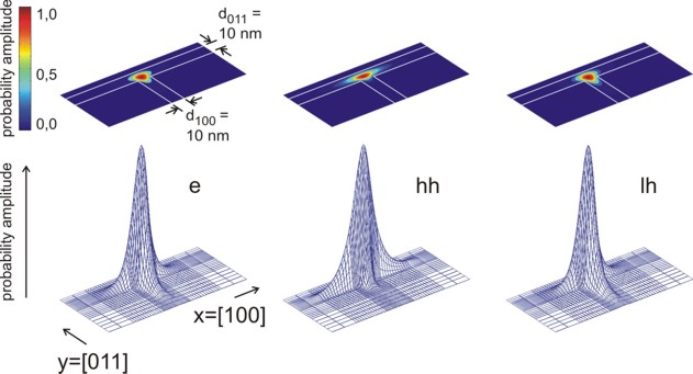
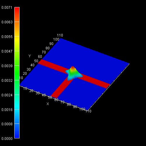
The following figures show the charge densities (Psi²; Psi =
wave function) of the ground states of the confined electron, heavy and light hole eigenstates
of the quantum wire.
|
 |
|
The probabiliy amplitudes of the electron (e),
the heavy hole (hh) and the light hole (lh) envelope functions at an
unstrained T-shaped intersection of two 10 nm wide GaAs quantum wells
embedded by Al0.35Ga0.65As barriers.
For the lower three pictures, the wave functions are normalized so that the
maximum of each equals one. |
|
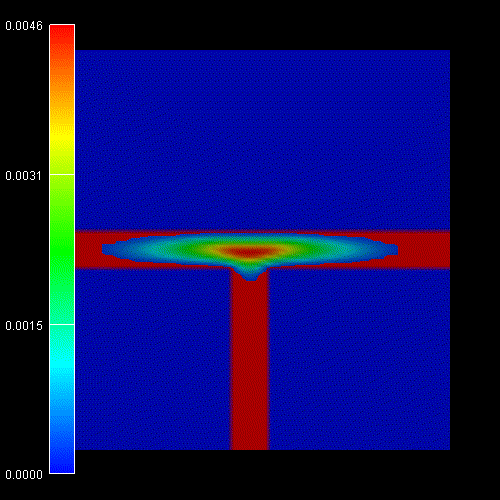
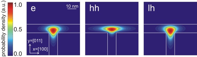 |
|
Contour diagram of the probabiliy amplitudes
of the electron (e), heavy hole (hh) and light hole (lh) eigenfunctions
(same figures as the ones above but this time viewed from the top).
One can clearly see that each ground state wave function is localized at the
T-shaped intersection and shows the T-shaped symmetry.
Due to the anisotropy of the heavy hole effective mass, the heavy hole
wave function prefers to extend along the [100] direction and hardly
penetrates into the quantum well that is aligned along the [011] direction.
The heavy hole mass along the [100] direction is only half as heavy as along
the [011] direction.
The light hole anisotropy is only minor and thus its symmetry resembles the
one of the isotropic electron.
Again, the normalization is chosen so that the maximum of the wave function
equals one. |
The quantum cluster ($quantum-regions)
used in this calculation has the size 108 nm x 108 nm. (The whole simulation area
is 110 nm x 110 nm.) The figures show an extract
of 60 nm x 60 nm.
The calculated eigenvalues are:
Single-band Schrödinger equation (effective-mass)
schroedinger-masses-anisotropic =
|
box |
yes |
no |
| electron ground state energy (eV) |
3.00584185 |
3.00584196 |
3.00582875 |
| heavy hole ground state energy (eV) |
1.45511017 |
1.45511001 |
1.45511013 |
| light hole ground state energy (eV) |
1.43906098 |
1.43906078 |
1.43906813 |
6-band k.p Schrödinger equation (6x6kp)
schroedinger-kp-discretization =
|
box-integration |
box-integration |
finite-differences |
kp-vv-term-symmetrization =
|
no |
yes |
yes |
| 1st hole energy (eV) (6-band k.p) |
1.4549 (2fold degenerate) |
- (2fold degenerate) |
- (2fold degenerate) |
| 2nd hole energy (eV) (6-band k.p) |
- (2fold degenerate) |
- (2fold degenerate) |
- (2fold degenerate) |
| 3rd hole energy (eV) (6-band k.p) |
- (2fold degenerate) |
- (2fold degenerate) |
- (2fold degenerate) |
| 4th hole energy (eV) (6-band k.p) |
- (2fold degenerate) |
- (2fold degenerate) |
- (2fold degenerate) |
| 5th hole energy (eV) (6-band k.p) |
- (2fold degenerate) |
- (2fold degenerate) |
- (2fold degenerate) |
Note:
- The grid lines have an equally spaced separation of 1 nm.
Choosing a denser gridding of 0.5 nm separation between 25 and 85 nm leads to
the following eigenvalues for box:
3.00529, 1.45525,
1.43942.
- Conduction band edge energy (GaAs) = 2.979 eV, hole band edge energy
(GaAs) = 1.459667 eV.
- Neumann boundary conditions were used. In case of confinement, the
wave function is zero at the quantum cluster boundaries.
(Here, schroedinger-masses-anisotropic = no
leads to the same results as the mixed derivatives d²/(dxdy) are zero
because our effective mass tensors are either isotropic (electrons) or oriented
with their principal axes parallel to the simulation system (holes).)
For these calculations, we neglected excitonic effects.
=> electron - heavy hole transition energy = 1.551 eV
=> electron - light hole transition energy =
1.567 eV
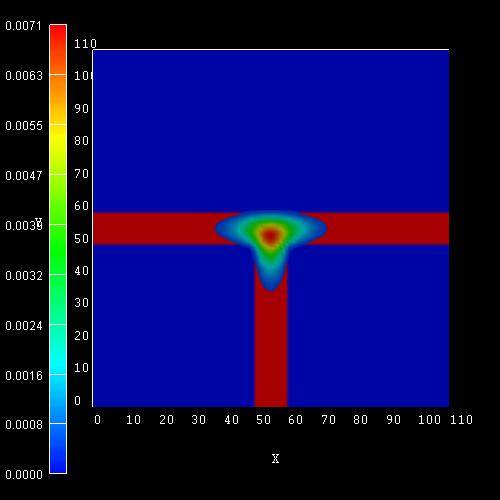
AVS/Express screenshots where the scale of the wave function (psi²) is given
in 1/nm². Integration of psi² over the simulation area of 110 * 110 nm² sums up
to one.
In addition to these ground states for kz=0, excited states are possible as well.
Similar to the subbands of a 1D quantum well that show a E(kx,ky)
dispersion one can assign a subband with the energy dispersion E(kz)
to each quantum wire eigenvalue which describes the free motion along the
quantum wire axis (z axis). A more advanced treatment would be to use k.p
theory to calculate the eigenvalues for different kz in order to
obtain the (nonparabolic) energy dispersion E(kz).
Understanding the meaning of the 6-band k.p parameters
For the same structure as above we perform the calculations again but this
time using 6-band k.p instead of single-band.
The left figure shows the wave function (psi²) for the hole ground state where
we used for GaAs the same Luttinger parameters as above:
gamma1 = 6.98, gamma2 = 2.06,
gamma3 = 2.93 (This corresponds to: L = -16.220,
 M
= -3.860
, N = -17.580)
The right figure shows the wave function (psi²) for the hole ground state where
we used for GaAs the Luttinger parameters
gamma1 = 6.98, gamma2 = 2.06 =
gamma3 (This corresponds to: L = -16.220, M
= -3.860, N = -12.36)
Choosing gamma2 = gamma3 corresponds
to an isotropic effective mass.
These results are in very good qualitative agreement with the heavy hole and
light hole wave functions calculated within the single-band approach. The impact
of an isotropic (for electrons and light holes) or anisotropic (for heavy hole)
effective mass tensor should now be clear.
 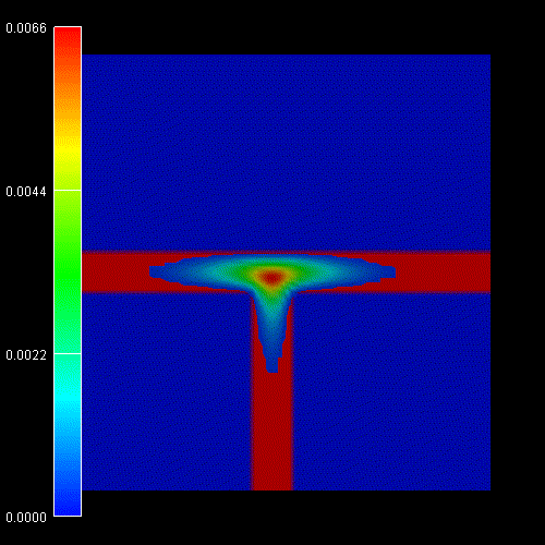
Within the 6-band k.p calculations we get only one confined hole state,
in contrast to the single-band effective-mass approach where we obtained one
confined state for the heavy hole and another confined state for the light hole.
Note: Here we used Dirichlet boundary conditions.
Interband transitions
(Note: This part has to be updated: Now we output the square of this matrix
element.)
We evaluate the spatial overlap integral between the electron and hole
envelope wave functions of the ground states. These numbers are proportional to
the transition probability. Additionally, the polarization of light has
to be taken into account to get the correct probability.
 $output-1-band-schroedinger

  ...

  interband-matrix-elements = yes
The results are contained in these files:
  Schroedinger_1band/interband2D_vb001_cb001_qc001_hlsg001_deg001_neu.dat
!
heavy hole <-> electron
  Schroedinger_1band/interband2D_vb002_cb001_qc001_hlsg002_deg001_neu.dat
! <-> electron
vb001: valence band 1, i.e. heavy
hole
vb002 1, i.e. heavy hole
cb001: conduction band 1, i.e.
electron for Gamma point
 heavy hole <-> Gamma conduction band


matrix element     transition energy e1-hh1

 ------------------------------------------------------------------

 <psi_vb001|psi_cb001>
0.9048
1.5507 eV
 light hole <-> Gamma conduction band


matrix element     transition energy e1-lh1

 ------------------------------------------------------------------

 <psi_vb001|psi_cb001>
0.9946
1.5668 eV
vb001: valence band hole state 1,
i.e. (heavy or light) hole ground state
cb0011, i.e.
electron ground state
By looking at the wave functions (psi²), one would expect a larger
overlap between the electron and the light hole rather than electron / heavy
hole.
As the calculatations show, this is exactly the case: The electron /
heavy hole overlap is only 0.9 whereas
the electron / light hole overlap is much larger:
0.99.
Note: A comparison of these results with different eigenvalue solvers and
discretization routines:
 heavy hole <-> Gamma conduction band


matrix element     transition energy e1-hh1

 ------------------------------------------------------------------

 <psi_vb001|psi_cb001>
-0.904760286602367 (box) 1.550732 eV


0.904842702923420 (yes) 1.550732 eV


0.904765324859528 (no)  1.550719 eV


(chearn,box)


0.556467704746565 (chearn,yes) 1.550732 eV -> imaginary part of psi is NOT zero


-0.904765324861447 (chearn,no)  1.550719 eV


-0.574566655967155 (arpack,box) 1.550732 eV -0.574531849467085 (bug fix
diag_sgV)


0.556467704746344 (arpack,yes) 1.550732 eV -> imaginary part of psi is NOT zero
-> complex arpack


0.904765324861290 (arpack,no)  1.550719 eV


0.904765324859528 (no,magnetic) 1.550719 eV -> imaginary part of psi is
zero


0.556442520299478 (chearn,no,magnetic) 1.550719 eV -> imaginary part of psi is
NOT zero


0.556442520299654 (arpack,no,magnetic) 1.550719 eV -> imaginary part of psi is
NOT zero -> complex arpack
 light hole <-> Gamma conduction band


matrix element     transition energy e1-lh1

 ------------------------------------------------------------------

 <psi_vb001|psi_cb001>
0.994609977897094 (box) 1.566781 eV


-0.994618620870019 (yes) 1.566781 eV


0.994618072678695 (no)  1.566761 eV


(chearn,box)


-0.579198621913980 (chearn,yes) 1.566781 eV -> imaginary part of psi is NOT zero


0.994618072678062 (chearn,no)  1.566761 eV


0.181672284480707 (arpack,box) 1.566781 eV 0.181668617064867 (bug fix diag_sgV)


0.665134365762336 (arpack,yes) 1.566781 eV -> imaginary part of psi is NOT zero
-> complex arpack


-0.994618072678148 (arpack,no)  1.566761 eV


0.994618072678695 (no,magnetic) 1.56676  eV -> imaginary part of psi
is zero


-0.579560683962475 (chearn,no,magnetic) 1.566761 eV -> imaginary part of psi is
NOT zero


-0.579560683962440 (arpack,no,magnetic) 1.56676  eV -> imaginary part of
psi is NOT zero -> complex arpack
See $output-1-band-schroedinger
for an explanation of this.
|