|
| |
nextnano3 - Tutorial
next generation 3D nano device simulator
2D Tutorial
I-V characteristics of an n-doped Si structure
1) n-doped Si
2) n-i-n-doped Si (n-doped, intrinsic, n-doped)
Author:
Stefan Birner
If you want to obtain the input files that are used within this tutorial, please
check if you can find them in the installation directory.
If you cannot find them, please submit a
Support Ticket.
1) -> Si_n_doped_1D_nn3.in

   -> Si_n_doped_2D_nn3.in


-> Si_n_doped_3D_nn3.in

2) -> Si_nin_doped_1D_nn3.in

   -> Si_nin_doped_2D_nn3.in


-> Si_nin_doped_3D_nn3.in
I-V characteristics of an n-doped Si structure
1) n-doped Si
- The structure we are dealing with consists of bulk Si that is sandwiched
between two contacts.
The whole structure has the following dimensions:
- along x axis: 20 nm (1 nm contact, 18 nm Si, 1 nm contact)
- along y axis: 5 nm
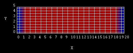
from left to right:
region-number = 1:  0 -  1 nm (blue)
  :
left contact
  region-number = 2:  1 - 19 nm (red)
  :
  region-number = 2: 19 - 21 nm (blue)
  :
- The Si is n-type doped with a donor concentration of ND = 1*1020 cm-3.
The energy level is 0.044 eV below the conduction band edge.
This leads to an electron density of n = 13.48 * 1018 cm-3.
This is the concentration of the ionized donors.
The Fermi level is taken to be at 0 eV in an equilibrium nextnano³ simulation
(EF = 0).
The distance of the conduction band from the Fermi level can be calculated
in the following way:
electron mass:
  conduction-band-masses = 0.156d0
    0.156d0  0.156d0 ! GAMMA: m,m,m


    1.420d0  0.130d0  0.130d0 ! L: ml,mt,mt


    0.916d0  0.190d0  0.190d0 ! X: ml,mt,mt
me = me*DOS = (ml·mt·mt)1/3
= (0.916·0.192)1/3 m0 = 0.321 m0
  conduction-band-degeneracies = 2 8 12
    !
valley degeneracy including spin degeneracy
Degeneracy of "X" valley ("X" = Delta in Si): 6
Spin degeneracy: 2
Nc = 12 (2 pi me
kBT / h² )3/2 = 12 (0.321 * 0.026 * 2.0886*1014)3/2
= 12 * 2.2816*1018 cm-3 = 2.737916*1019 cm-3
(identical to nextnano³ result)
(Gamma and L valley: NcGamma = 1.54615994*1018
cm-3 NcL = 1.55494502*1019
cm-3)
Holes: Nvhh = 9.87481457*1018 cm-3
Nvlh = 1.50177430*1018 cm-3
Nvso = 2.84047719*1018 cm-3
Note that heavy and light holes are degenerate for k = 0.
=> Nv = Nvhh
+ Nvlh = 1.137658887*1019 cm-3
The Semiconductor equation: np = ni2 = Nc Nv exp(
- Egap/kBT) = Nc
1.1377*1019 cm-3 exp( - 1.095/0.026) = 1.23792*1020
cm-6
Egap = 1.095 eV
ni = 1.11262*1010 cm-3
p = ni²/n = 9.1845 cm-3
| Maxwell-Boltzmann |
Fermi-Dirac |
| n (T) = Nc(T) exp(
(EF - Ec) / (kBT) ) |
n (T) = Nc(T) F1/2(
(EF - Ec) / (kBT) ) |
| p (T) = Nv(T) exp(
(Ev - EF) / (kBT) ) |
p (T) = Nv(T) F1/2(
(Ev - EF) / (kBT) ) |
| |
F1/2 = Fermi-Dirac integral of order 1/2 multiplied by
2/SQRT(pi) (i.e. F1/2 includes
the Gamma prefactor) |
When using the Maxwell-Boltzmann statistics as an approximation we obtain
for Ec:
Ec = kBT ln (Nc / n) = 0.026 eV * ln (
2.737916*1019 cm-3 / (13.47836*1018 cm-3))
= 0.026 eV * ln 2.031 = 0.0183 eV
=> Note: Inside the code we make use of the Fermi-Dirac integrals (Fermi-Dirac
statistics). nextnano³ result: 0.01385
eV
The distance of the valence band from the Fermi level can be calculated in
the following way:
Ev = - kBT ln (Nv / p) = - 0.026 * 42.538 =
- 1.099
(Maxwell-Boltzmann statistics approximation)
=> Note: Inside the code we make use of the Fermi-Dirac integrals (Fermi-Dirac
statistics). nextnano³ result: -1.08148
eV
- The mobility model that is applied is called
mobility-model-simba-2. It is described here:
$mobility-model-simba
The calculated electron mobility is:
- at 0.00 V: 64.5 cm²/Vs
- at 0.20 V: 52.9 cm²/Vs
In our example the mobility does neither depend on the temperature (T = T0
= 300 K) nor on the perpendicular electric field (E_|_
= 0). If E_|_ /= 0 we would have to use
mobility-model-simba-2e instead, in order to take
into account the dependence on the perpendicular electric field.
Therefore the equation for the electron mobility reduces to:
at 0.00 V:
µ = µmin
+ µdop
/ (1 + ((ND + NA)
/ Nref
) a_dop) =
= 55.2 cm²/Vs + 1374.0 cm²/Vs / (1 + (1*1020 cm-3)
/ 1.072*1017 cm-3) 0.73 ) = 64.47
cm²/Vs
  $mobility-model-simba

   material-name  = Si
   !
taken from
SIMBA
manual
   n-alpha-doping = 0.73d0   !
  [---]
n-N-ref-doping = 1.072d17 ! [1/cm^3]
   n-mu-min       =
  55.2d0   ! [cm^2/Vs]
   n-mu-doping    = 1374.0d0
  ! [cm^2/Vs]
$end_mobility-model-simba
- We sweep the voltage at the right contact and calculate the current
density for 0.00 V, 0.02 V, 0.04 V, ..., 0.20 V (
10
steps).
  $voltage-sweep

   sweep-number
  = 1

   sweep-active
  = yes       ! 'yes'/'no'

   poisson-cluster-number  = 2
  !
right contact
   step-size
  = 0.02d0    ! < 0.1 V

   number-of-steps         =
  10

   data-out-every-nth-step = 1

  $end_voltage-sweep
Results
- The current-voltage (I-V) characteristic can be found in the following
file:
IV_characteristics2D.dat (2D)
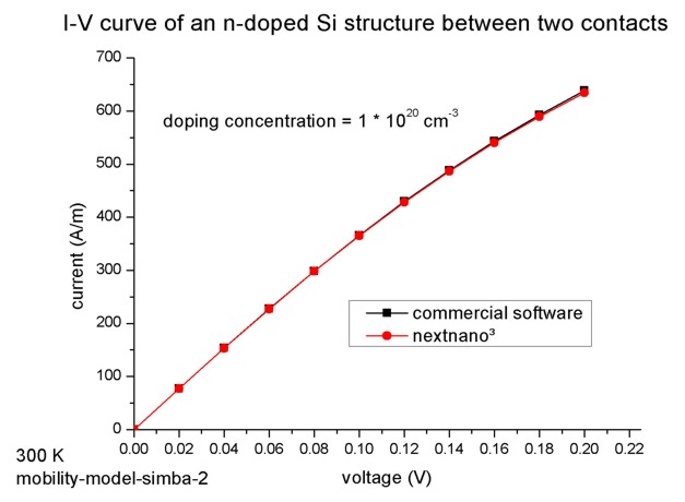
The nextnano³ results match perfectly to the I-V characteristics obtained with a
commercial software package.
The units for the current in a 2D simulation are [A/m].
Dividing this two-dimensional current value by the width of the device (in our
case 5 nm) we obtain the current in units of [A/m²] which is the usual unit of
a 1D simulation.
As our simple 2D example structure is basically equivalent to a 1D structure
we can easily compare our 2D results with the 1D results to check for
consistency. It is also possible to perform a 3D simulation. In this case, the
units for the three-dimensional current are [A]. Dividing by the area of the
device of 25 nm², we obtain the 1D units of [A/m²].
The 1D and 3D input files are:
1DSi_n_doped.in, 3DSi_n_doped.in
| voltage |
current [A/m]
(nextnano³ 2D) |
current [A/m²]
(nextnano³ 2D results
divided by the width 5 nm) |
current [A/m²]
(nextnano³ 1D results) |
current [A]
(nextnano³ 3D results) |
current [A/m²]
(nextnano³ 3D results
divided by the square 5x5 nm²) |
0 |
0 |
0 |
0 |
0 |
0 |
0.04 |
153.3 |
3.066 * 1010 |
3.064
      * 10
10 |
0.766
* 10-6 |
3.064
* 1010 |
0.08 |
298.1 |
5.962 * 1010 |
5.961
      * 10
10 |
1.490
* 10-6 |
      5.961
      * 10
10 |
0.12 |
428.1 |
8.562 * 1010 |
8.566
      * 10
10 |
2.141
* 10-6 |
      8.566
      * 10
10 |
0.16 |
540.5 |
1.081 * 1011 |
1.081 * 1011 |
2.704
* 10-6 |
1.081
      * 10
11 |
0.20 |
634.7 |
1.269
      * 10
11 |
1.270
      * 10
11 |
3.175
* 10-6 |
1.270
      * 10
11 |
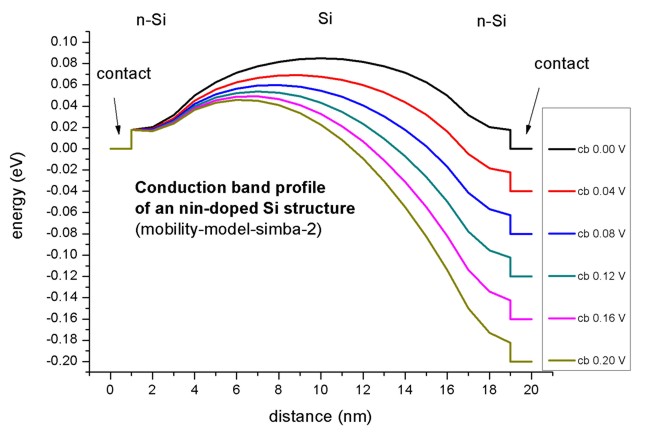
2) n-i-n-doped Si (n-doped, intrinsic, n-doped)
- This is a similar structure as in 1).
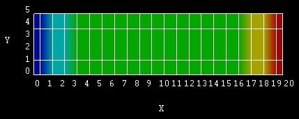
from left to right:
region-number = 1:  0 -  1 nm
  (dark blue)  :
left contact
  region-number = 2:  1 -  3 nm (bright
  blue):
  region-number = 3:  3 - 17 nm (green)
  :
  region-number = 4: 17 - 19 nm (yellow)
  :
  region-number = 5: 19 - 21 nm (red)
  :
To take into account the doping profile properly we define separate region
clusters for the n-doped regions. (For more details on how
to set accurate grid lines for a doping profile, confer
$doping-function).
Most of the Si region is now undoped (intrinsic) (x = 3 - 17 nm).
Only the Si region next to the two contacts is n-type doped (x = 1 - 3 nm, x =
17 - 19 nm). The doping concentration is the same as in 1).
- We will compare two different mobility models:
- mobility-model-simba-0
(no dependence on electric field)
- mobility-model-simba-2
$mobility-model-simba
Results
- The current-voltage (I-V) characteristic can be found in the following
file:
IV_characteristics2D.dat (2D)
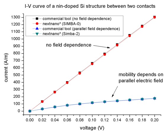
The nextnano³ results match perfectly to the I-V characteristics obtained with a
commercial software package.
mobility-model-simba-0
does not include a dependence of the mobility on the parallel electric
field, thus the current is proportional to the applied voltage.
mobility-model-simba-2
takes into account a dependence of the mobility on the parallel
electric field. In this case the current is smaller because the mobility
decreases when the applied voltage increases.
The units for the current in a 2D simulation are [A/m].
Dividing this two-dimensional current value by the width of the device (in our
case 5 nm) we obtain the current in units of [A/m²] which is the usual unit of
a 1D simulation.
As our simple 2D example structure is basically equivalent to a 1D structure
we can easily compare our 2D results with the 1D results to check for
consistency. It is also possible to perform a 3D simulation. In this case, the
units for the three-dimensional current are [A]. Dividing by the area of the
device of 25 nm², we obtain the 1D units of [A/m²].
The 1D and 3D input files are:
1DSi_nin_doped.in, 3DSi_nin_doped.in
Again, the nextnano³ 1D and 3D results are in agreement with the nextnano³
2D results.
- The following figure shows the conduction band profile (
band_structure/cb1D_003_ind*.dat)
for different voltages.
|