| nextnano.com nextnano³ Download | Search | Copyright | Publications * password protected |
nextnano³ software
|
|
| 1D GaN/AlGaN QW dispersion |
|
|
|
|
|
nextnano3 - Tutorialnext generation 3D nano device simulator1D Tutorialk.p dispersion of an unstrained GaN QW embedded between strained AlGaN layersAuthor: Stefan Birner If you want to obtain the input files that are used within this tutorial, please
check if you can find them in the installation directory. k.p dispersion of an unstrained GaN QW embedded between strained AlGaN layersThis tutorial is based on:
[0001] growth direction
Calculation of the electron and hole energies and wave functions for k|| = 0.
The structure consists of a 3 nm unstrained GaN quantum well, embedded between 8.4 nm strained Al0.2Ga0.8N barriers. The AlGaN layers are strained with respect to the GaN substrate. The GaN quantum well is assumed to be unstrained. The structure is modeled as a superlattice (or multi quantum well, MQW), i.e. we apply periodic boundary conditions to the Poisson equation. The growth direction is along the hexagonal axis, i.e. along [0001].
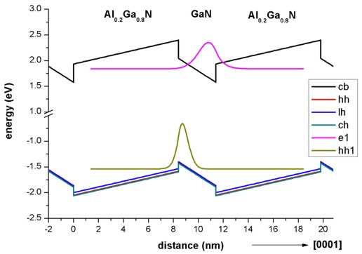
Conduction and valence band profileThe following figure shows the conduction and valence (heavy hole, light hole and crystal-field split-off hole) band edges of our structure, including the effects of strain, piezo- and pyroelectricity. The ground state electron and the ground state heavy hole wave functions (psi2) are shown. Due to the built-in piezo- and pyroelectric fields, the electron wave function are shifted to the right and the hole wave function to the left (Quantum Confined Stark Effect, QCSE).
StrainThe strain inside the GaN quantum well layer is zero. The output of the strain tensor can be found in this file:
Piezoelectric polarizationThe piezoelectric polarization for the [0001] growth direction is zero inside
the GaN QW (because the strain is zero in the QW). The output of the piezoelectric interface charges can be found in this file:
Pyroelectric polarizationThe pyroelectric polarization for the [0001] growth direction is -0.029
inside the GaN QW. The output of the pyroelectric interface charges can be found in this file:
Poisson equationSolving the Poisson equation with periodic boundary conditions (to mimick the
superlattice) leads to the following electric fields: The output of the electrostatic potential (units [V]) and the electric field
(units [kV/cm]) can be found in these files:
Schrödinger equationThe following figure shows the electron and hole wave functions (psi2) of the GaN/AlGaN structure for k|| = 0. The heavy and light hole wave functions are very similar in shape. In agreement with the paper
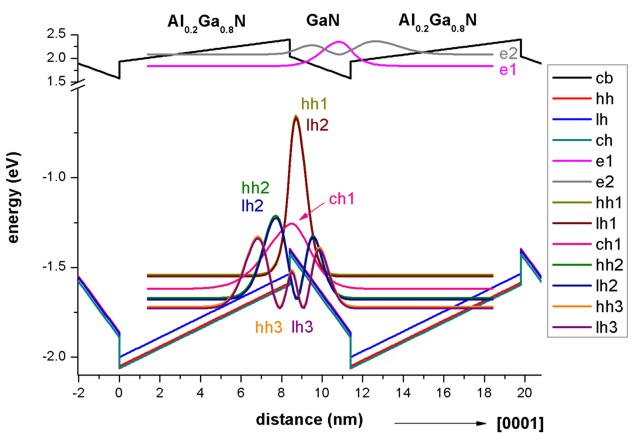
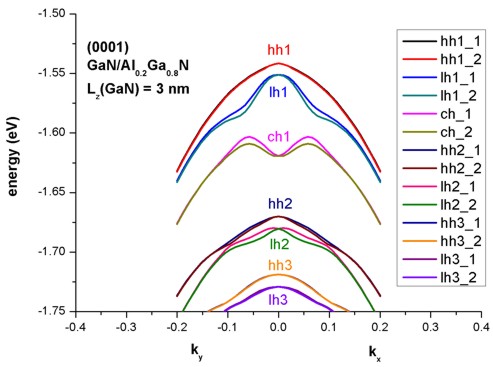
k|| dispersion: Calculation of the electron and hole energies and wave functions for k|| /= 0.
The grid has a spacing of 0.1 nm leading to a sparse matrix of dimension 1050 which has to be solved for each k|| point for the eigenvalues (and wave functions). We chose as input: Due to symmetry arguments, we solved the the Schrödinger equation only for
the k|| points along the line (kx > 0, ky = 0),
i.e. we had to solve the Schrödinger equation 22 times (i.e. to calculate the
eigenvalues of a 1050 x 1050 matrix 22 times).
Because our quantum well is not symmetric (due to the piezo- and
pyroelectric fields!), the eigenvalues for spin up and spin down are not
degenerate any more. They are only degenerate at k|| = 0.
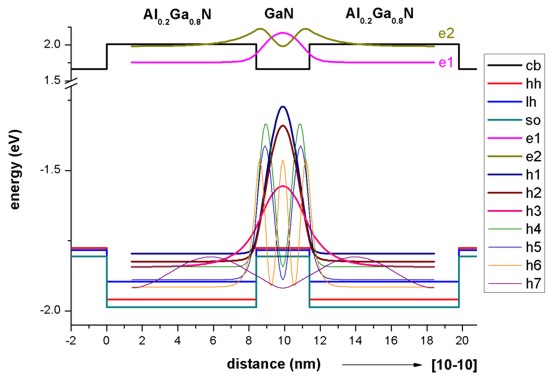
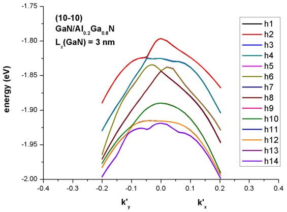
[10-10] growth direction (m-plane)
If one grows the quantum well along the [10-10] growth direction, then the
pyroelectric and piezoelectric fields along the [10-10] direction are zero. The following figure shows the electron and hole wave functions (psi2)
of the (10-10)-oriented GaN/AlGaN QW for k|| = 0. In agreement with the paper
k|| dispersion: Calculation of the electron and hole energies and wave functions for k|| /= 0.
Due to the symmetry of the quantum well, we expect degenerate eigenvalues for
the in-plane dispersion relation (Kramers degeneracy).
|
|
|