Hello World
- Input Files:
basics_1D_hello_world.in
- Scope of the tutorial:
The general structure of the input files
Running the input file with nextnanomat
Basic content of the simulation output
Defining 1D structures
Computing basic band profiles
- Introduced Keywords:
global{ temperature simulate1D{} substrate{ name } crystal_zb{ x_hkl y_hkl } }
grid{ xgrid{ line{ pos spacing } }
structure{ region{ binary{ name } contact{ name } everywhere{} line{ x } } }
contacts{ fermi{ name bias } }
classical{ Gamma{} HH{} LH{} output_bandedges{ averaged } }- Relevant output Files:
bias_00000\bandedges.dat
The input file basics_1D_hello_world.in is prepared to compute a band profile of a simple 1D structure consisting of an InAs layer sandwiched between two GaAs layers without strain, see Figure 2.5.2.1.
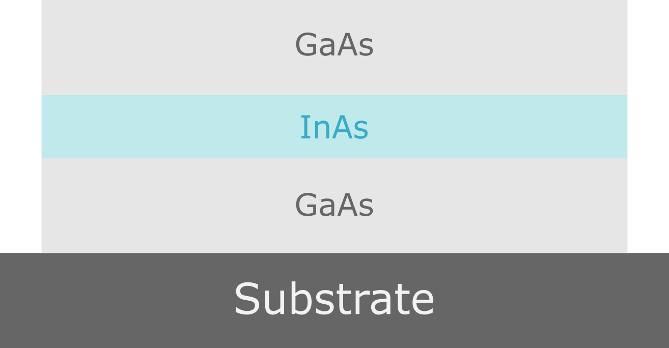
Figure 2.5.2.1 A schematic of a GaAs/InAs/GaAs heterostructure
Global Settings of the Simulation
The group global{} is required to define multiple general aspects of whole simulation.
The temperature of the crystal and carriers is set to 300 K by setting temperature = 300.
The band gap is temperature dependent by default.
Choosing that the simulation is held in 1D space is done by calling simulate1D{}.
The substrate is chosen by a nested group substrate{ name = "GaAs"}, where name is an
attribute to which you can assign any of the available material names.
In this case the choice of substrate material is arbitrary, because strain calculations are not triggered.
Crystal orientation in the simulation coordinate system is defined inside a nested group crystal_zb{}
setting values of two attributes: x_hkl = [100] and y_hkl = [010],
which assigns [100] direction to the x-axis of the simulation (the axis of the 1D simulation)
and [010] direction to the y-axis of the simulation (still existing).
 5global{ # this group is required in every input file
 6    temperature = 300           # set temperature (required)
 7    simulate1D{}                # choose between 1D, 2D or 3D simulation
 8    substrate{ name = "GaAs" }  # substrate material (required)
 9    crystal_zb{                 # crystal orientation
10        x_hkl = [1, 0, 0]       # x-axis is perp. to lattice plane (100)
11        y_hkl = [0, 1, 0]       # y-axis is perp. to lattice plane (010)
12                                # z-axis is determined from x-axis and y-axis
13    }
14}
Numerical Grid
The group grid{ } is used to define the numerical grid of the simulation.
As there is only x-axis in the 1D simulations, only xgrid{ } group is used to define the grid.
Each group line{} defines a “line” (a point in 1D, a line in 2D, and a plane in 3D) at a position pos
forcing a grid spacing spacing in its vicinity and assuring that there is a grid point
at the specified coordinate pos.
16grid{ # this group is required in every input file
17    xgrid{                  # grid in x direction
18        line{
19            pos = 0.0       # start of device at x=0.0 nm
20            spacing = 4.0   # grid spacing 4.0 nm
21        }
22                            # from x=0.0 nm to x=20.0 nm further grid points
23                            # are created according to the interpolated spacing (4.0 -> 0.5)
24                            # (no equidistant grid spacing)
25        line{
26            pos = 20.0      # grid point at GaAs/InAs interface
27            spacing = 0.5   # grid spacing 0.5 nm
28        }
29                            # from x=20.0 nm to x=30.0 nm further grid points
30                            # are created according to the interpolated spacing (0.5 -> 0.5)
31                            # (equidistant grid spacing)
32        line{
33            pos = 30.0      # grid point at InAs/GaAs interface
34            spacing = 0.5   # grid spacing 0.5 nm
35        }
36                            # from x=30.0 nm to x=50.0 nm further grid points
37                            # are created according to the interpolated spacing (0.5 -> 4.0)
38                            # (no equidistant grid spacing)
39        line{
40            pos = 50.0      # end of device at x=50.0 nm
41            spacing = 4.0   # grid spacing 4.0 nm
42        }
43    }
44}
There are 4 “lines” specified in the input file. The two of them with pos = 0.0 and pos = 50.0, as the most outer ones,
define the span of the entire grid. The remaining two, with pos = 20.0 and pos = 30.0, are defined at the positions
of material interfaces defined in the next group, to assure stable representation of the design in the discrete grid space.
The figure Figure 2.5.2.2 shows schematically the process of defining the grid.

Figure 2.5.2.2 Schematics of the simulation grid with four “lines” defined (red circles). Interpolated grid points between lines are depicted with black circles.
One can also view the grid spacing using nextnanomat, see Figure 2.5.2.3.
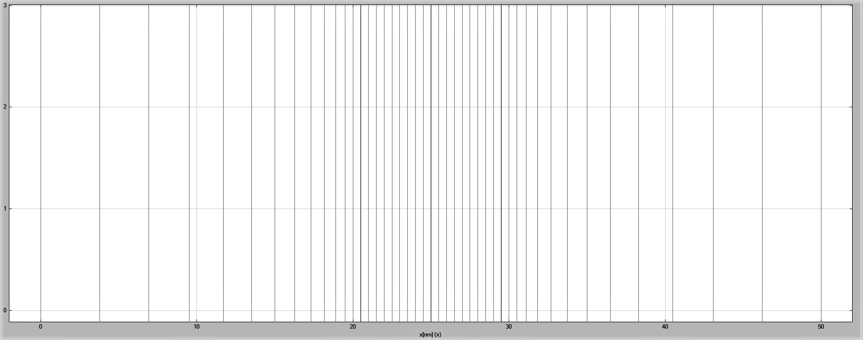
Figure 2.5.2.3 The numerical grid in the simulation.
Defining the Structure
The definition of specific structure is kept in the group structure{}.
Here groups region{} are used to assign binary materials (using binary{})
and boundary conditions for Poisson and current equations (using contact{}) to specific
regions within the earlier defined space.
First, material GaAs and boundary condition named “whatever” are assigned to entire space
by specifying binary{ name = GaAs }, contact{ name = whatever }, and everywhere{}
inside one region{}.
Next, material InAs is assigned to a region spanning from \(x=20.0\) to \(x=50.0\),
by defining another region{} group, containing binary{ name = InAs } ` and :code:`line{ x = [ 20.0, 30.0 ] }.
In that case, InAs is overwriting GaAs in the selected region,
while the boundary conditions specified by contact{} remain.
46structure{ # this group is required in every input file
47    region{
48        binary{ name = GaAs }               # material GaAs
49        contact{ name = hello_world }       # contact definition
50        everywhere{}                        # ranging over the complete device, from x=0.0 nm to x=50.0 nm
51    }
52    region{
53        binary{ name = InAs }               # material InAs
54        line{ x = [ 20.0, 30.0 ] }          # overwriting previously defined GaAs in the interval x=20.0 nm to x=30.0 nm
55}
Bondary conditions
The boundary conditions for Poisson and current equations are specified in the group contacts{}.
They have to be specified even if the equations are not solved.
Here, the boundary condition for quasi-Fermi levels only is chosen by calling fermi{}.
The contact is named “hello_world” by setting name = hello_world.
This name is used for referencing to this specific contact in the definition of the structure.
The energy of Fermi level is set to 0 eV by setting bias = 0.0.
58contacts{ # this group is required in every input file
59    fermi{                                  # type of contact
60        name = hello_world                  # refer to regions with contact name 'hello_world'
61        bias = 0.0                          # region with contact name 'hello_world' is set to 0 V
62    }
63}
Choice of Bands
The classical{} group is called to choose which bands should be taken into account
in the semiclassical simulations, here only computing the profile.
The first conduction band at \(\Gamma\) point, heavy-, and light-hole valence bands are selected
by calling groups: Gamma{}, HH{}, and LH{}, respectively.
The group output_bandedges{} allows to output the band profile,
while its attribute averaged = no ensures that the profile is not going to be averaged
over neighboring grid points in the output file.
65classical{ # this group is required in every input file
66    Gamma{}                                 # include conduction band at gamma point in the calculation
67    HH{}                                    # include heavy hole band in the calculation
68    LH{}                                    # include light hole band in the calculation
69    output_bandedges{ averaged = no }       # necessary to see a energy profile
70}
Running the Simulation and Viewing the Results
The simulation can be started in nextnanomat by pressing F8 on the keyboard or by clicking the icon  .
A folder with simulation results is created in the output directory.
.
A folder with simulation results is created in the output directory.
The output of the simulation can be viewed under the “Output” tab at the top of nextnanomat.
Within the tab, navigate to the folder bias_00000 and click on bandedges.dat.
A plot of the Gamma, LH and HH energy profiles should be visible.
The grid used in the simulation can be shown by checking the box “Show grid”
in the menu on the left of nextnanomat.
To export the figure as a .plt file, click on the  icon in the top right corner.
Then click on bandedges.dat. Hold down shift on the keyboard and click the plots of your interest.
In this tutorial, Gamma[eV], HH[eV] and LH[eV] are chosen from the bottom right panel.
Press shift + a on the keyboard or the  icon in the top right corner of nextnanomat.
Next, select  icon at the top and choose the option “Create and Open Gnuplot File (*.plt) from Items of Overlay”.
A Gnuplot window should pop up. Click the
icon at the top and choose the option “Create and Open Gnuplot File (*.plt) from Items of Overlay”.
A Gnuplot window should pop up. Click the  icon and name the file, and save it.
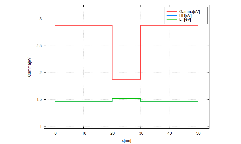
Figure 2.5.2.4 Energy profile of GaAs/InAs/GaAs heterostructure without considering strain.
Last update: nn/nn/nnnn