Constant Doping
Attention
This tutorial is under construction
- Input Files:
basics_1D_doping_constant_p.in
basics_1D_doping_constant_np.in
Introduction
This tutorial is the third in our introductory series. We want to show the general framework of adding doping to material regions in nextnano++. After completing this tutorial, you will know more about
adding doping to material regions
specify the species (donor/ acceptor)
Keywords: doping{}, impurities{}, donor{}, acceptor{}
Main
As an overview, Figure 2.5.2.10 shows the two structures that will be created in this tutorial.
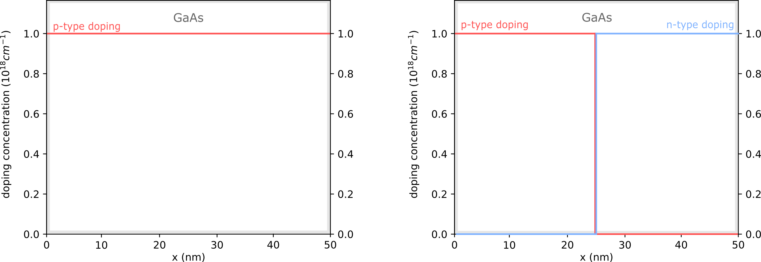
Figure 2.5.2.10 shows p-doped GaAs (left) and p-doped/ n-doped GaAs (right).
The Basics I: Adding doping to bulk material
As an introductory example to doping, we want to n-dope a single GaAs layer as shown on the left of Figure 2.5.2.10. You can use the template input file basics_1D_doping_constant_p.in.
Specifying regions with dopants
38structure{ # this group is required in every input file
39    output_impurities{ boxes = yes}             # output doping concentration [10^18 cm-3]
40
41    region{
42        binary{ name = GaAs }                   # material: GaAs
43        contact{ name = whatever }              # contact definition
44        everywhere{}                            # rangeing over the complete device, from x=0.0 nm to x=50.0 nm
45
46        doping{                                 # add doping to the region
47            constant{                           # constant doping concentration profile
48                name = "Custom_impurity_name"   # name of impurity
49                conc = 1.0e18                   # doping concentration [cm-3]
50            }
51        }
52    }
53}
First of all, we create just one thick GaAs layer. Then we add doping to the exact same region by the specifier doping{}. Inside doping{}, we have to
set the doping profile. Here we choose to have constant doping concentration over the whole region. Inside constant{} we specify name and doping concentration (conc)
for this region. The name is arbitrary, and you can choose whatever name you like. By giving the doping a reference name, we can select the species and electronic properties for this doping
later inside the group impurities{}.
Since we want to inspect the doping concentration distribution for every grid point in the output,
the flag boxes = yes inside output_impurities{} is active.
Specify impurity species
54impurities{ # if doped regions exist, this group is required
55    acceptor{                           # select the species of dopants
56        name = "Custom_impurity_name"   # select doping regions with name = "Custom_impurity_name"
57        energy = 0.045                  # ionization energy of dopants [eV]
58        degeneracy = 4                  # degeneracy of dopants
59    }
60}
If dopants are added to any region, the group impurity{} has to be included in the input file. acceptor{} sets
the species for regions with name “Custom_impurity_name”. We further refine the properties by setting ionization energy (energy) and degeneracy level (degeneracy).
Output
We simulate the device by clicking F8 on the keyboard. In the related output folder
you should find a plot of the concentration profile (\(\Rightarrow\) Structure \(\Rightarrow\) density_acceptor.dat) as shown in Figure 2.5.2.11.
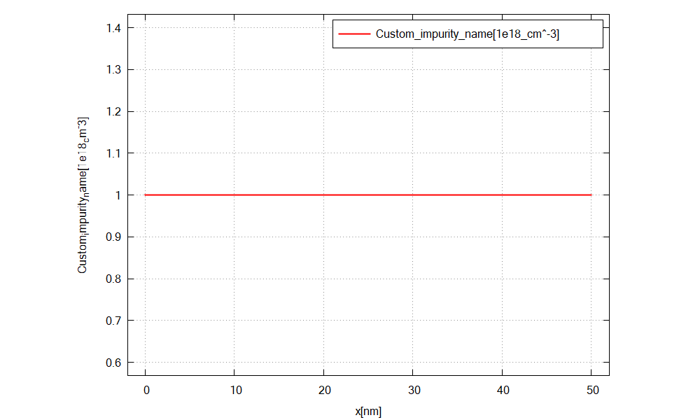
Figure 2.5.2.11 shows the doping concentration of acceptors along the x direction.
The Basics II: Adding different doping to bulk material (p-n junction)
As another introductory example, we n-dope the first half and p-dope the second half of the single GaAs layer as in Figure 2.5.2.10 (right). Now, the doping regions do not coincide with the material regions. We have to define material and doping regions separately. You can use the template input file basics_1D_doping_constant_np.in.
Specifying regions with dopants
42structure{ # this group is required in every input file
43    output_impurities{ boxes = yes}     # output doping concentration [10^18 cm-3]
44
45    region{
46        binary{ name = GaAs }           # material: GaAs
47        contact{ name = whatever }      # contact definition
48        everywhere{}                    # ranging over the complete device, from x=0.0 nm to x=50.0 nm
49    }
50
51    region{                             # separate region for adding doping only (no material is specified)
52        line{ x = [ 0.0, 25.0 ] }       # position: x=0.0 nm to x=25.0 nm
53        doping{                         # add doping to the region
54            constant{                   # constant doping concentration profile
55                name = "p-type"         # name of impurity
56                conc = 1.0e18           # doping concentration [cm-3]
57            }
58        }
59    }
60
61    region{                             # separate region for adding doping only (no material is specified)
62        line{ x = [ 25.0, 50.0 ] }      # position: x=25.0 nm to x=50.0 nm
63        doping{                         # add doping to the region
64            constant{                   # constant doping concentration profile
65                name = "n-type"         # name of impurity
66                conc = 1.0e18           # doping concentration [cm-3]
67            }
68        }
69    }
70}
In the code above, we first create a bulk GaAs layer and then add two doping regions for n-type and p-type dopants. The doping regions do
not include a material specification. Inside these regions, the position (line{}) and the doping (doping{}) is specified.
The dopants are added to the previously defined material region.
In fact, this example illustrates that, as far as the initialization is concerned, nextnano++ treats doping and materials separately.
Specify impurity species
73impurities{ # if doped regions exist, this group is required
74    donor{                  # select the species of dopants
75        name = "n-type"     # select doping regions with name = "n-type"
76        energy = 0.045      # ionization energy of dopants
77        degeneracy = 2      # degeneracy of dopants
78    }
79    acceptor{               # select the species of dopants
80        name = "p-type"     # select doping regions with name = "p-type"
81        energy = 0.045      # ionization energy of dopants [eV]
82        degeneracy = 4      # degeneracy of dopants
83    }
84}
As we already know if dopants are added, the group impurity{} has to be included in the input file. Apart from acceptor{}, we introduce
donor{} as another doping species. For both species we refine the properties here.
Output
We simulate the device by clicking F8 on the keyboard. In the related output folder
you should find a plot of the concentration profiles (\(\Rightarrow\) Structure \(\Rightarrow\) density_acceptor.dat / density_donor.dat)
as shown in Figure 2.5.2.12 and Figure 2.5.2.13.
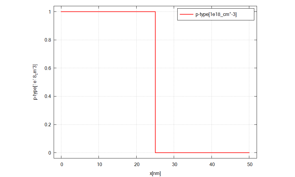
Figure 2.5.2.12 shows the doping concentration of acceptors along the x direction (p-doped region).
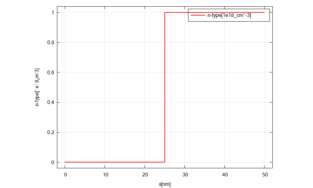
Figure 2.5.2.13 shows the doping concentration of donors along the x direction (n-doped region).
Important things to remember
dopants are part of a region, i.e. structure{…region{…doping{}…}…}. Here you determine the concentration of one impurity type for each grid point.
The impurity type (species and properties) are defined inside the group impurity{}
Last update: nn/nn/nnnn