5.14.2. Silicon MOS Capacitor
- Files for the tutorial located in nextnano++\examples
MOS_CV_5 nmSiO2_5 nmCont_Dop1e16_QM_1D_fine_grid.nnp
MOS_CV_5 nmSiO2_5 nmCont_Dop1e16_QM_1D.nnp (nonuniform grid)
MOS_CV_5 nmSiO2_5 nmCont_Dop1e16_QM_2D.nnp
MOS_CV_5 nmSiO2_5 nmCont_Dop1e16_QM_2D_periodic_x.nnp (uniform grid along x direction with periodic boundary conditions, quasi-1D simulation)
- References
[Goetzberger] A. Goetzberger, M. Schulz, Fundamentals of MOS Technology, In: H. J. Queisser (eds) Festkörperprobleme 13, Advances in Solid State Physics 13, Springer, Berlin, Heidelberg, 309-336 (1973), https://doi.org/10.1007/BFb0108576
[Wu] Y.-C. Wu, Y.-R. Jhan, 3D TCAD Simulation for CMOS Nanoeletronic Devices, Springer, Singapore (2018)
[Sze] S. M. Sze, K. K. NG, Physics of Semiconductor Devices (3rd ed.), John Wiley, New York (2007)
[Brews] J. R. Brews, W. Fichtner, E. H. Nicollian, S. M. Sze, Generalized guide for MOSFET miniaturization, IEEE Electron Device Letters 1, 2 (1980) https://doi.org/10.1109/EDL.1980.25205
[Miura-Mattausch] M. Miura-Mattausch, H. J. Mattausch, N. D. Arora, C. Y. Yang, MOSFET modeling gets physical, IEEE Circuits and Devices Magazine 17, 29 (2001) https://doi.org/10.1109/101.968914
Contents
In this part we discuss and compare the effect of different mobility models on the output characteristics of the MOSFET and how they affect properties such as pinch-off, saturation, etc.
2D MOS Capacitor
In this tutorial we illustrate the simulation and analysis of an N-channel MOSFET (Metal-Oxide-Semiconductor Field-Effect Transistor) in 2D as implemented in CMOS technologies and nanodevice fabrication. The first step in simulating the MOSFET is the construction and the simulation of the corresponding MOS capacitor, i.e. the Metal-Oxide-Semiconductor device, which can act as a capacitor on its own, and is an integral part of the MOSFET. The gate contact on this capacitor is the same gate contact as of the MOSFET, and it underlies the same physics in both the MOS and the MOSFET. The 2D sketch of the MOS capacitor is illustrated in the following figure Figure 5.14.2.1
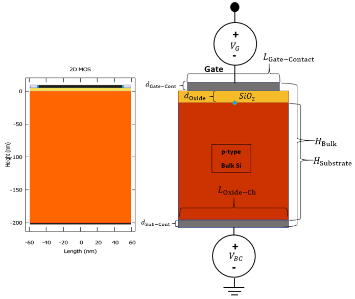
Figure 5.14.2.1 The geometry of the 2D MOS design, and its equivalent geometry from the output file regions.vtr (colored differently in post-processing). The blue circle indicates the position of the origin of our \((x,y)\) coordinate system.
In this tutorial we use a p-doped bulk-Si MOS with a Schottky contact at the gate (instead of a poly-Si contact), and ohmic contact at the substrate. Therefore, the effect of poly-Si depletion at the gate is not present in either of the devices in order to produce the C-V characteristics of our capacitor, which then is the same MOS device used within the N-Ch MOSFET. The bulk p-doping level is \(1 \times 10^{16} \mathrm{cm^{-3}}\), and the oxide layer which consists of SiO:sub:2 has a thickness of \(d_{\mathrm{ox}} = 5 {\mathrm{nm}}\). The length of the channel is \(L_{\mathrm{G}}=100 {\mathrm{nm}}\), the substrate has a height of \(H_{\mathrm{Substrate}} = 200 {\mathrm{nm}}\). The importance of the C-V characteristics of the MOS device derives from the fact, that the charge inversion layer, that is responsible for conduction in the MOSFET, is generated by the capacitive properties of the MOS devices.
Low-Frequency Capacitance
In what follows are the results of our numerical calculations. Concretely, we solve the coupled Schrödinger, Poisson and current equations in two dimensions. We compare our results with the analytic formulas given in standard text books.
The low-frequency capacitance of a MOS capacitor can be measured experimentally with a low frequency signal. In the simple case scenario, the interface trapped charges (charges trapped in the oxide) usually play no role in the capacitance of the device and are not considered in our simulations. Therefore the total capacity of the device is a series connection of the oxide capacitance and the depletion layer capacitance,
The oxide capacitance is the capacitance of the oxide layer, which is independent of the bias, and is simply calculated according to \(C_{\mathrm{ox}} = \varepsilon_{\mathrm{ox}}/d_{\mathrm{ox}}\). This gives a capacitance per unit area (\({\mathrm{F}}/{\mathrm{cm}}^2\)). Multiplying this value with the length \(L_{\mathrm{G}}\) and width \(W\) of the gate gives a capacitance in units of \(\mathrm{F}\).
The depletion layer capacitance is calculated using the charge in the depletion layer as defined in equation (5.14.2.2),
where \(W_{\mathrm{D}}\) is the width of the depletion layer, \(\varepsilon_{\mathrm{s}}\) is the dielectric constant of the semiconductor and \(\varepsilon_{\mathrm{ox}}\) the dielectric constant of the oxide. The depletion layer capacitance is then given by the derivative \(\partial Q_{\mathrm{D}}/\partial \psi_{\mathrm{s}}\), where \(\psi_{\mathrm{s}}\) is the surface potential. Further details on the surface potential can be found in the appendix section. Therefore, the total capacitance calculated according to these formulas would approximately approach the \(C_{\mathrm{ox}}\) at its maximum, would have a flat-band capacitance \(C_{\mathrm{FB}}\) given by the expression in equation (5.14.2.3) , i.e. the capacitance at the voltage, which creates the flat-band condition in the MOS band structure,
with \(L_{\mathrm{D}}\) as the Debye screening length. The Debye length for our MOS capacitor amounts to \(\approx 40.8 {\mathrm{nm}}\), and with that the flat-band capacitance is calculated to be \(C_{\mathrm{FB}} \approx 1.85 {\mathrm{mF/m}^2}\), the equivalent of \(1.85 {\mathrm{pF/cm}}\) if the channel length is \(100 {\mathrm{nm}}\). The C-V curve of the MOS, taking the entire substrate for charge integration, with \(\partial Q_{\mathrm{Sub}} / \partial V_{\mathrm{Bias}}\) is shown in figure Figure 5.14.2.3. Note that the output of the simulations, however, is only the total charge (per cm in 2D), as shown in figure Figure 5.14.2.2, which needs to be (first multiplied with the elementary charge \(|q|\), and then) derived with respect to the bias voltage:
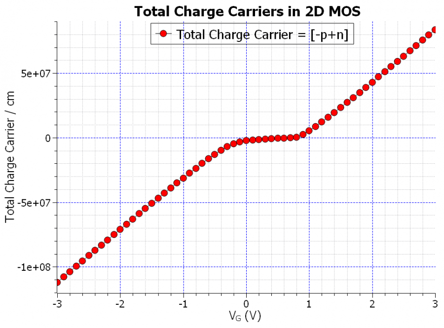
Figure 5.14.2.2 The total charge carriers per cm of the MOS, integrated in the substrate, vs. the applied gate bias.
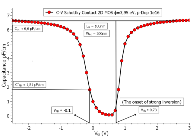
Figure 5.14.2.3 The C-V characteristics of the 2D MOS with \(N_{\mathrm{Sub}}=10^{16} {\mathrm{cm}^{-3}}\) doping concentration in the p-doped silicon substrate, channel length of 100 nm, a Schottky barrier of \(\phi_{\mathrm{B}} = 3.95 {\mathrm{eV}}\), and a charge integration region equal to the entire substrate. (Note that the flat-band voltage has been chosen from the observation of the band edges in the simulation output, which are flat for the bias value of \(-0.1 {\mathrm{V}}\)).
In the above figure the \(C^{*}_{\mathrm{FB}}\) is marked with * because the value measured differs from the calculated value. Later we will show how the C-V curve could be measured, so that the value of the flat-band capacitance is consistent with (5.14.2.3).
There are three values which we read from the graph (actually four but since we have the band edges here in the simulation output, we just need three). The first is the oxide capacitance \(C_{\mathrm{ox}}\), which is approximately the ceiling of the curve. The second is the flat-band capacitance \(C_{\mathrm{FB}}\), corresponding to the value of the flat-band voltage \(V_{\mathrm{FB}}\) (read from the status of the band edges in the simulation output). And the third is the threshold voltage \(V_{\mathrm{Th}}\), which is the onset of the strong inversion. The flat-band condition in the 1-dimensional band edges output is illustrated in figure Figure 5.14.2.4:
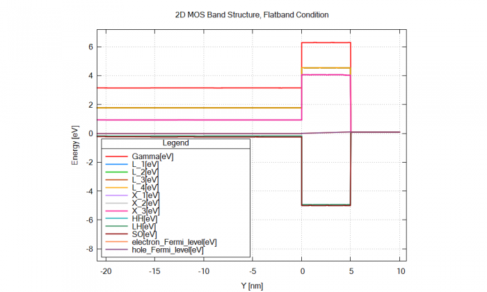
Figure 5.14.2.4 The alignment of conduction and valence band edges with respect to the Fermi levels of the 2D MOS under the flat-band condition along a one-dimensional slice along the y direction. (The lowest conduction band edge is labeled with X.
The bias voltage that results in a band structure in the figure Figure 5.14.2.4, is called the flat-band voltage \(V_{\mathrm{FB}}\). This voltage is related to, and is a part of the definition of the threshold voltage,
The \(\psi_{\mathrm{B}}\) is the distance of the semiconductor Fermi level to the mid-point of the band gap, and it is estimated that the onset of the strong inversion is at the point when the surface potential \(\psi_{\mathrm{s}} \approx 2\psi_{\mathrm{B}}\). This surface potential is estimated to be
Calculating this expression for our system, the surface potential amounts to \(\approx 0.713 {\mathrm{V}}\), while the expression \(\sqrt{4\varepsilon_{\mathrm{Si}}qN_{\mathrm{Sub}}\psi_{\mathrm{B}}}/C_{\mathrm{ox}} \approx 0.073 {\mathrm{V}}\), which is actually the voltage drop across the oxide layer \(V_{\mathrm{ox}}\). Therefore taking the flat-band voltage \(V_{\mathrm{FB}} = -0.1 {\mathrm{V}}\), we arrive at a threshold voltage \(V_{\mathrm{Th}} \approx 0.7 {\mathrm{V}}\), which is somewhat lower than the \(0.73 {\mathrm{V}}\) read from the curve. Indeed the value of the threshold voltage is strongly affected by the value of the Schottky barrier.
The height of the Schottky barrier used here, however, has to reflect the metal-SiO:sub:2 interface barrier, and not the metal-semiconductor barrier. This barrier depends on the metal and its work function that is used, and is therefore different for different metals. It is also mentioned in [Wu], that “the work function of the metal gate has to be properly defined in order to achieve the expected threshold voltage \(\mathbf{V_{\mathrm{Th}}}\)”. Even though that the barrier heights for metals such as aluminum have been reported to be around \(3.15 {\mathrm{eV}}\), the barrier height of metals such as gold (Au), and silver (Ag), have been reported to be around \(4.0 {\mathrm{eV}}\) [Goetzenberger]. Here, in order to arrive at a threshold voltage of \(0.7 \mathrm{V}\), the barrier had to be chosen \(3.95 \mathrm{eV}\).
The Schottky Barrier, Doping Concentration, Depletion Region
In the following part we look at a set of figures, which illustrate various parameter changes, which then lead to variations in the three important values which we want to read from the C-V curve. First would be the threshold voltage, and the flatband voltage, both of which could be influenced by the height of the Schottky barrier, and the doping concentration in the bulk-semiconductor, as figure Figure 5.14.2.5 illustrates:
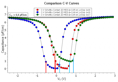
Figure 5.14.2.5 The comparison of the C-V characteristics of the 2D MOS for varying Schottky barrier and the substrate doping concentration, and their effects on the threshold voltage (vertical blue lines), and the flatband voltage (vertical red lines)
As it could be seen in the above figure Figure 5.14.2.5, both the barrier height and the doping concentration shift the threshold voltage \(V_{\mathrm{Th}}\), and the flatband voltage \(V_{\mathrm{FB}}\), however the flatband voltage is more affected by the barrier height rather than the doping concentration. It is also worth mentioning, that the doping concentration alone also affects the minimum capacitance in both low-frequency regime, and the high frequency regime, namely \(C_{\mathrm{min}}\), and \(C^{'}_{\mathrm{min}}\), which are the bottom limits of the C-V curve (\(C^{'}_{\mathrm{min}}\) is directly inversely related to the maximum depletion region width, and apparently so is the \(C_{\mathrm{min}}\)).
In the next set of figures we see, how changing the charge integration region can affect the C-V curve, which then would answer why the \(C^{*}_{\mathrm{FB}}\) in our original curve did not exactly match the calculated flatband capacitance \(C_{\mathrm{FB}}\). The following figure Figure 5.14.2.6, illustrates the effect of changing the charge integration region on the flatband capacitance \(C_{\mathrm{FB}}\):
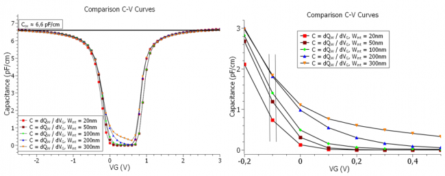
Figure 5.14.2.6 The comparison of the C-V characteristics of the 2D MOS for varying the width of the charge integration region.
And figure Figure 5.14.2.7 shows the C-V curve of the MOS capacitor for a charge integration region of \(W_{\mathrm{int}}=300 {\mathrm{nm}}\):
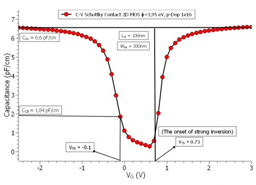
Figure 5.14.2.7 The comparison of the C-V characteristics of the 2D MOS for varying the width of the charge integration region.
Now it seems that the value of the flatband capacitance \(C_{FB}\) in the C-V curve (\(1.84 \mathrm{pF/cm}\)) agrees very well with the calculated value. The reason for that is that, as mentioned in equation (5.14.2.2), the charge in the depletion region is directly proportional to the width of the depletion region. This width has a maximum which is given by:
which turns out to be \(\approx 303 {\mathrm{nm}}\) in our MOS capacitor. Therefore, it should be noted, that in order to be able to reach the flatband capacitance defined by the formalism, the charge integration region should be greater or equal to the maximum depletion region width \(W_{\mathrm{D},max}\). Note that the charge carrier integration has to be specifically mentioned as a region with the following flags in the <structure{ }_integrate> group:
region{
    rectangle{ # Si Charge Carrier Integration Zone
       x = [-$L_Oxide_Ch/2 , :remove_enter:
       $L_Oxide_Ch/2]
       y = [-$H_Substrate, 0]
    }
    binary{
       name = "Si"
    }
 integrate{
       electron_density{}         # n-charge carriers
       hole_density{}             # p-charge carriers
       label = "Si_Substrate"
     }
 }
The total charge is then \(q(-p_{\mathrm{tot}}+n_{\mathrm{tot}})\). The derivative of this charge with respect to the voltage bias sweep results in the C-V curve, as mentioned before.
Appendix: 2D MOS
The MOS capacitor is a 2D device in its correct form for simulations (with the optional 3rd dimension if need be…). The width of the substrate needs to be somewhat larger than the channel length, so that the depletion layer charges have enough space to expand, also the boundary conditions have to be set to non-periodic in the simulation. That is because even though the channel length is set by the length of the gate-contact, and the inversion layer is bounded by this length, this is not the case for the charges in the depletion layer. Figure Figure 5.14.2.8 illustrates this phenomenon:
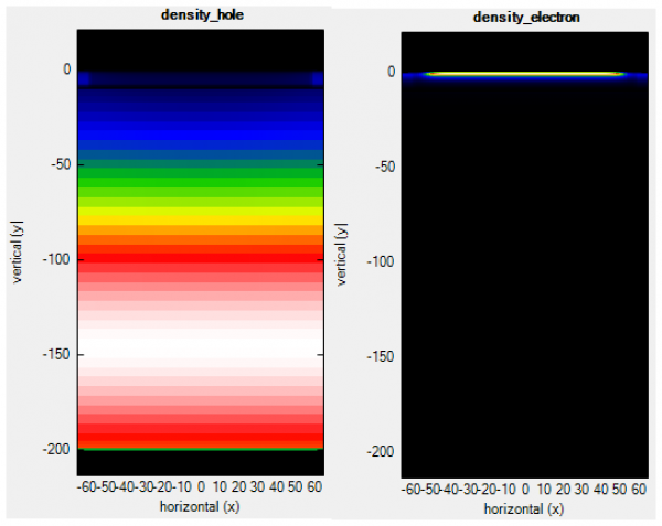
Figure 5.14.2.8 The spatial distribution of charge carriers (electrons) in the inversion layer during inversion, compared to the ones (holes) in the depletion region during depletion.
If we set the substrate width to the length of the channel, which basically would mean that the MOS could also be simulated in 1D, the C-V curve would look like the following in figure Figure 5.14.2.9
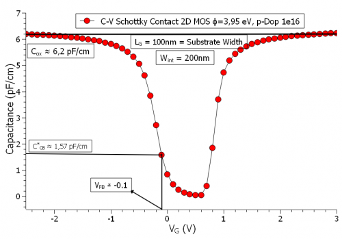
Figure 5.14.2.9 The C-V curve of the quasi 1-D Simulations of the MOS (this is when we set the length of the oxide and the channel-length equal in a 2D simulation and set the boundary condition in x-direction as periodic).
As seen in the C-V curve, not only the oxide capacitance \(C_{\mathrm{ox}}\) is somewhat less than what it should be, the flatband capacitance \(C_{FB}\) (\(1.57 {\mathrm{pF/cm}}\)) does not agree, within an acceptable margin of error, with the calculated value.
With regards to the surface potential \(\psi_{\mathrm{s}}\), it is worth mentioning, that this potential can be measured by measuring the electrostatic potential at the semiconductor-oxide interface, as function of the gate-voltage. For that in nextnano++, one needs to perform a bias sweep at the gate-contact using the template, and make a 1D-section slice of the simulation in the section{ } group, mentioning a range in y-direction around \(y=0\), so that exactly one grid point falls within this range:
output{
  section1D{                 # output a 1D section of the simulation area (1D slice)
    name = "surface_potential"              # name of section enters file name
    x = 0
    range_y = [-0.2, 0.0]    # 1D slice at x = 0 through the middle of the channel
                                            # however limited to the range in y
  }
}
Using the post-processing in the template, one can then construct a curve, which should look like the one shown in figure Figure 5.14.2.10
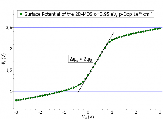
Figure 5.14.2.10 The surface potential, at the semiconductor-oxide interface \(\psi_{\mathrm{s}}\), as a function of the gate.voltage \(V_{\mathrm{G}}\)
Such a curve would go through the origin for an ideal MOS device, however depending on how the electrostatic potential is calculated at the contacts, this curve could go higher or lower on the y-axis. The transition from accumulation to strong inversion of the total capacitance happens basically in the region of the potential, where the line is drawn, for which \(\Delta \psi_{s} \approx 2 \psi_{B}\).
The last remark regarding the capacitance of the MOS could be that, even though the classical formula of parallel plates capacitor is also here applied to the oxide capacitance, in small dimensions and in few nanometer regime, other effects such as tunneling current, and thermionic emissions could play a significant role. Additionally, since the quantum mechanical charge distribution distances itself from the semiconductor-oxide interface (as we shall see in the inversion layer comparison of the MOSFET), these effects would significantly reduce the maximum capacitance of the MOS. As we could see from the C-V curve the flatband capacitance is less than \(30 \%\) of the oxide capacitance, even though one would expect that the \(C_{\mathrm{FB}}\) be somewhere around \(80 \%\) of the \(C_{\mathrm{ox}}\). Therefore if the aforementioned effects be taken under consideration, it could very well be that the \(C_{\mathrm{ox}}\) fall to half of its parallel-plate value.
Last update: 2025-10-28